Vishay Semiconductor Opto Division TFDU6103-TR3
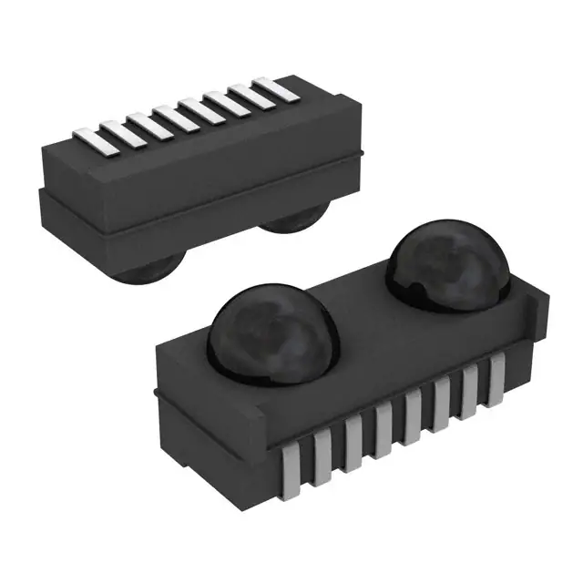
- Part No.:
- TFDU6103-TR3
- Manufacturer:
- Vishay Semiconductor Opto Division
- Category:
- IrDA Transceiver Modules
- Package:
- Datasheet:
-
TFDU6103-TR3.pdf
- Description:
- TXRX IRDA 4MBIT 4MM SIDE 8-SMD
- Quantity:
- Payment:

- Shipping:

Inventory:1,651
Please send an inquiry. Send us your inquiry, and we will respond immediately.
Product details
Overview
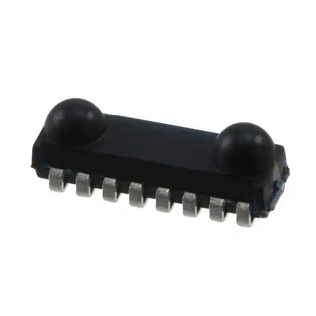
TFDU6103-TR3 from Vishay Semiconductors is a fast infrared (FIR) transceiver module compliant with IrDA® physical layer standards, supporting 4 Mbit/s data rates and carrier-based remote control up to 2 MHz. It integrates a PIN photodiode, infrared emitter (IRED), and low-power CMOS control IC in a surface-mount BabyFace package (9.7 mm × 4.7 mm × 4 mm), enabling compact IR communication in portable computing and consumer electronics.
For engineers reviewing the TFDU6103-TR3 datasheet, TFDU6103-TR3 pinout, TFDU6103-TR3 application, or TFDU6103-TR3 equivalent, key selection considerations include its dual-voltage supply architecture (VCC1/VCC2), tri-state RXD output with weak pull-up in shutdown, IrDA-compliant link distance ≥1 m (±15°), remote control range up to 22 m, and eye safety Class 1 certification per IEC 60825-1.
Technical Context
The TFDU6103-TR3 implements a split-power-supply architecture: VCC1 powers the receiver and logic, while VCC2 independently drives the IRED anode-enabling optimized current control and reduced load on the regulated supply. Its mode switching is controlled via SD and TXD inputs, with a falling edge on SD latching TXD state to select SIR (≤115.2 kbit/s), MIR (≤1.152 Mbit/s), or FIR (4 Mbit/s) bandwidth modes.
Internally, it features a CMOS-controlled IRED driver with built-in pulse width limitation (max 150 μs), optical rise/fall times ≤40 ns, and stochastic jitter ≤20 ns at 4 Mbit/s. The receiver includes automatic gain control and threshold detection referenced to 0.5×VCC1, with sensitivity specified as minimum irradiance of 80–90 mW/m² for FIR operation at 4 Mbit/s.
Key Specifications
| Parameter | Value and Actual Design Meaning |
|---|---|
| Data Rate | 4 Mbit/s FIR compliant with IrDA® Physical Layer v1.1+, enabling high-speed short-range wireless data transfer between portable devices |
| Supply Voltage Range | 2.4 V to 5.5 V on VCC1; separate VCC2 up to 6.5 V for IRED drive-supports flexible power system partitioning |
| Idle Supply Current | <3.3 mA in receive mode (MIR/FIR), enabling battery-sensitive applications like PDAs and handheld cameras |
| Shutdown Current | <1 μA over full temperature range (−25 °C to +85 °C), critical for ultra-low-power standby states |
| Link Distance | ≥1 m at ±15° field-of-view per IrDA spec, with window losses tolerated-validates robustness in real-world enclosures |
| Transmitter Wavelength | Typ. 886 nm (range 875–900 nm), compatible with both IrDA communication and standard RC protocols (e.g., Philips RC5/RC6®) |
| Eye Safety Class | Class 1 per IEC 60825-1:2001, enforced by LED current control and limited on-time-no external safety interlocks required |
Pinout & Package
TFDU6103-TR3 uses a side-view surface-mount BabyFace package measuring 9.7 mm × 4.7 mm × 4 mm (MSL4, lead-free qualified). Pin numbering follows standard 8-pin DIP-style layout with GND at pin 8 and NC at pin 7.
| Pin/Terminal | Circuit Role | Design Meaning |
|---|---|---|
| 1 - VCC2 | IRED anode supply | Dedicated unregulated input for IRED drive; supports external resistor for >3.6 V operation to limit internal power dissipation |
| 2 - IRED | IRED cathode | Internally connected to driver transistor; forms current path with VCC2 for pulsed IR emission |
| 3 - TXD | Transmit data input | CMOS-level serial input; on-chip protection disables IRED if asserted >100 μs-prevents LED damage during firmware faults |
| 4 - RXD | Received data output | Push-pull CMOS output; no external pull-up needed; floats with 500 kΩ weak pull-up to VCC1 in shutdown mode |
| 5 - SD | Shutdown & mode select | Active-high shutdown; falling edge samples TXD to set receiver bandwidth (SIR/MIR/FIR)-enables dynamic speed negotiation |
| 6 - VCC1 | Transceiver core supply | Powers receiver amplifier, comparator, logic, and RXD driver; independent of VCC2 for noise isolation |
| 7 - NC | No connect | Not internally bonded; must remain unconnected per design-no routing or grounding allowed |
| 8 - GND | Signal reference ground | Primary ground reference for all analog and digital circuitry; pin 8 defines voltage reference for all other pins |
Key Features
| Feature | Design Value |
|---|---|
| Split power supply architecture | VCC1 (receiver/logic) and VCC2 (IRED anode) decouple noise-sensitive analog paths from high-current IR drive |
| Tri-state RXD with weak pull-up | Enables bus sharing without contention; floating output in shutdown avoids unintended logic states during power sequencing |
| Programmable bandwidth mode switching | SD/TXD sequence selects SIR/MIR/FIR modes dynamically-eliminates need for hardware configuration jumpers |
| Integrated eye safety compliance | Class 1 per IEC 60825-1 enforced by controlled LED current, limited on-time, and single-fault immunity-reduces system-level safety certification burden |
| EMI immunity without shielding | Immune to >550 V/m RF fields across 700–2000 MHz (GSM/3G bands), verified without external metal shielding-simplifies mechanical design |
Applications
| Mobile Computing Interfaces | Digital Imaging Devices |
|---|---|
Use Scenario: Bidirectional file transfer between notebook PCs and PDAs using IrDA FIR protocol. IC Role / Device Role / Timing Role: Full-duplex infrared transceiver handling 4 Mbit/s serial data framing, modulation/demodulation, and optical signal conditioning. Use Value: Enables cable-free synchronization of contacts, calendars, and media files with <1 m line-of-sight range and ±15° angular tolerance-validated per IrDA physical layer spec. |
Use Scenario: Remote control and image metadata exchange between DSLR cameras and wireless flash triggers. IC Role / Device Role / Timing Role: Dual-mode IR interface operating in FIR for high-speed EXIF tag transfer and carrier-based mode for legacy RC command signaling. Use Value: Supports 886 nm wavelength compatibility with both IrDA receivers and standard RC photodiodes-enables single-hardware platform for data + control functions. |
| Consumer Electronics Peripherals | Industrial Data Collection Terminals |
Use Scenario: Infrared printing and fax transmission in compact all-in-one office devices. IC Role / Device Role / Timing Role: Low-latency (40–100 μs) transceiver managing burst-mode document data transfer with automatic gain control for variable ambient light. Use Value: Delivers reliable link performance at ≥1 m despite enclosure window attenuation-meets IrDA spec even with polycarbonate lens losses. |
Use Scenario: Wireless barcode scanner-to-host communication in warehouse handheld terminals. IC Role / Device Role / Timing Role: Ruggedized IR front-end providing ESD >1 kV and latch-up immunity >100 mA for industrial EMI environments. Use Value: Maintains operation under 550 V/m RF interference (GSM/3G bands) without shielded enclosures-reducing BOM cost and assembly complexity. |
Equivalent & Alternatives
The following parts are listed as comparable options for similar infrared transceiver applications.
| Alternative Part | Technical Difference | Application Difference | Selection Advice |
|---|---|---|---|
| Vishay TFDU6300-TT3 | Top-view mounting variant (vs. TFDU6103-TR3 side-view); identical electrical specs and pinout; same BabyFace package footprint but rotated orientation | Requires PCB layout revision for top-emission optics; suitable where sensor alignment favors vertical beam path over horizontal | Select when optical path geometry mandates top-emitting configuration-mechanical fit differs, but firmware and interface remain drop-in compatible |
| Vishay TFBS4650-TR1 | Single-function IR receiver (no transmitter); 38 kHz carrier demodulator only; no TXD, VCC2, or IRED pins; smaller 3.5 mm × 2.8 mm × 1.8 mm package | Limited to remote control reception only; cannot support bidirectional IrDA data links or FIR/MIR protocols | Choose only for receive-only use cases like TV remotes-lacks transceiver functionality, so not a functional substitute for TFDU6103-TR3 in full-duplex systems |
Compared with TFDU6103-TR3, the TFDU6300-TT3 offers identical performance in a top-view orientation-ideal for revised mechanical layouts-while the TFBS4650-TR1 is a receive-only device with no transmit capability, making it unsuitable for any IrDA data communication requirement.
Availability
TFDU6103-TR3 is available at Aetrix Electronics and suitable for mobile computing interfaces, digital imaging devices, consumer electronics peripherals, and industrial data collection terminals requiring stable component supply and long-term lifecycle support.
Supply support for TFDU6103-TR3 includes scheduled delivery planning, volume procurement assistance, BOM continuity management, traceable sourcing, and lifecycle availability coordination for OEM customers, industrial embedded developers, connected-device designers, and electronics production programs.
Manufacturer
Vishay Semiconductors is a global leader in discrete semiconductors and passive components, specializing in high-reliability optoelectronics, power management, and sensing solutions for industrial, automotive, and consumer markets.
The TFDU6103-TR3 belongs to Vishay's BabyFace infrared transceiver family, designed specifically for space-constrained, low-power IrDA-compliant wireless data links in portable electronics-balancing optical performance, regulatory compliance, and surface-mount manufacturability.
FAQ
What is the primary function of the TFDU6103-TR3?
The TFDU6103-TR3 is a fully integrated fast infrared (FIR) transceiver module supporting 4 Mbit/s IrDA data communication and carrier-based remote control up to 2 MHz. It combines a PIN photodiode, infrared emitter (IRED), and low-power CMOS control IC in a single BabyFace surface-mount package. Its role is to enable bidirectional optical data transfer in portable electronics such as notebooks, PDAs, and digital cameras-making TFDU6103-TR3 essential for cable-free short-range connectivity where RF is restricted or undesirable.
How does the TFDU6103-TR3 handle power supply separation between receiver and transmitter?
The TFDU6103-TR3 uses two independent supply pins: VCC1 powers the receiver, logic, and RXD output driver, while VCC2 supplies the IRED anode. This split architecture isolates high-current IRED switching noise from sensitive analog receiver circuitry, improving signal integrity and reducing EMI coupling. For VCC2 >3.6 V, an external current-limiting resistor is recommended to manage internal power dissipation-ensuring stable operation across the full 2.4 V to 5.5 V VCC1 range and up to 6.5 V on VCC2. This design directly benefits TFDU6103-TR3 implementations in noise-sensitive portable systems.
Can the TFDU6103-TR3 operate in both IrDA and standard remote control modes?
Yes, the TFDU6103-TR3 supports dual-mode operation: IrDA-compliant FIR (4 Mbit/s), MIR (1.152 Mbit/s), and SIR (≤115.2 kbit/s) data communication, plus carrier-based remote control up to 2 MHz. Its 886 nm peak emission wavelength (875–900 nm range) satisfies both IrDA spectral requirements and legacy RC protocols like Philips RC5/RC6®. Remote control range exceeds 8 m (typ. 22 m), validated under standard conditions. This dual capability makes TFDU6103-TR3 suitable for converged devices needing both high-speed data sync and universal remote functionality-without requiring separate IR components.
What is the significance of the "Not for New Designs" notice on the TFDU6103-TR3 datasheet?
The "Not for New Designs" designation indicates that Vishay has discontinued active development and marketing of the TFDU6103-TR3 for future product introductions, though it remains available for existing production programs. This status reflects strategic portfolio rationalization-not obsolescence-and does not affect current technical specifications, reliability, or supply chain support. Aetrix Electronics maintains inventory and lifecycle coordination for TFDU6103-TR3 to serve ongoing manufacturing needs, including BOM continuity management and traceable sourcing. Customers designing new systems should evaluate newer Vishay alternatives like the TFDU6300 series, but TFDU6103-TR3 remains fully viable for sustaining engineering and legacy program support.
How does the TFDU6103-TR3 ensure eye safety compliance?
The TFDU6103-TR3 achieves Class 1 eye safety per IEC 60825-1:2001 through three integrated design measures: precise LED current control, strict limitation of IRED on-time, and inherent single-fault immunity-no external safety circuitry is required. Its optical output radiant intensity is capped at 468 mW/sr (at 0°), and exposure limits are enforced by internal timing logic that prevents continuous emission beyond safe thresholds. This certification allows direct integration into consumer products without additional optical safety barriers or user warnings-reducing time-to-market and certification overhead for TFDU6103-TR3-based designs.
TFDU6103-TR3 Specifications
- Product attributes
- Attribute value
- Manufacturer:
- Vishay Semiconductor Opto Division
- Series:
- -
- Packaging:
- Tape & Reel (TR)
- Product Status:
- Obsolete
- Data Rate:
- 4Mbs (FIR)
- Voltage - Supply:
- 2.4 V ~ 5.5 V
- Idle Current, Typ @ 25°C:
- 2 mA
- Link Range, Low Power:
- 1m
- Orientation:
- Side View
- Operating Temperature:
- -25°C ~ 85°C
- Size:
- 9.7mm x 4.7mm x 4.0mm
- Standards:
- IrPHY 1.4
- Shutdown:
- Yes
TFDU6103-TR3 FAQ
1.How can I place an order for TFDU6103-TR3 through Aetrix?
Please submit a Request for Quotation (RFQ) for TFDU6103-TR3 on Aetrix. Our sales agent will provide a competitive quotation and guide you through the order confirmation once you accept the terms.
2.Are the price and stock information for TFDU6103-TR3 reliable?
The price and inventory of TFDU6103-TR3 are updated periodically and may fluctuate due to market conditions. Stock and pricing data are typically refreshed every 24 hours. Quotation validity for TFDU6103-TR3 is usually 5 days.
3.What payment methods are accepted for TFDU6103-TR3?
We accept Wire Transfer, PayPal, Credit Card, Western Union, MoneyGram, and Escrow for TFDU6103-TR3 transactions.
Note: Certain payment methods may incur a processing fee.
4.How is shipping managed for TFDU6103-TR3?
TFDU6103-TR3 orders can be shipped via leading logistics carriers, including DHL, UPS, FedEx, TNT, or Registered Mail.
Once your TFDU6103-TR3 order is processed, you will receive an email with the shipment details and tracking number.
Note: Tracking information may take up to 24 hours to appear. Express delivery typically takes 3–5 business days.
5.How can I obtain technical support or documentation for TFDU6103-TR3?
For technical support, including TFDU6103-TR3 datasheets, pinout diagrams, or application guidance, please contact our engineering support team. They can provide detailed documentation and assistance for your TFDU6103-TR3 requirements.
6.How does Aetrix verify that TFDU6103-TR3 is sourced from the original manufacturer or authorized distributors?
All TFDU6103-TR3 products on Aetrix are procured from qualified distributors and authorized channels. Our dedicated quality assurance team conducts strict verification, including traceability checks and, if necessary, third-party testing. This ensures that TFDU6103-TR3 meets industry standards.
7.What is the process for return or replacement of TFDU6103-TR3?
All TFDU6103-TR3 units undergo pre-shipment inspection (PSI). If there is an issue with TFDU6103-TR3, returns or replacements are accepted under the following conditions:
1.Quantity discrepancies, incorrect items, or visible external defects (such as breakage or corrosion), acknowledged by Aetrix.
2.The issue is reported within 90 days of delivery.
3.The TFDU6103-TR3 part is unused and in its original packaging.
Return procedure for TFDU6103-TR3:
1.Submit a request within 90 days.
2.Obtain a Return Material Authorization (RMA) from Aetrix.
TFDU6103-TR3 Tags
-
TFBS4650-TR1
Vishay Semiconductor Opto Division
-
TFBS4711-TT1
Vishay Semiconductor Opto Division
-
TFBS4650-TT3
Vishay Semiconductor Opto Division
-
TFBS4711-TR1
Vishay Semiconductor Opto Division
-
TFDU4101-TR3
Vishay Semiconductor Opto Division
-
TFDU4101-TT3
Vishay Semiconductor Opto Division
-
TFDU4301-TR1
Vishay Semiconductor Opto Division
-
TFDU4301-TT3
Vishay Semiconductor Opto Division
-
TFDU4301-TT1
Vishay Semiconductor Opto Division
-
TFBS4652-TR1
Vishay Semiconductor Opto Division
-
TFBS4711-TR3
Vishay Semiconductor Opto Division
-
TFBS4652-TT1
Vishay Semiconductor Opto Division
Tech Hub

Comparator circuit design covering voltage thresholds, input limits, open-collector outputs, LM393 wiring, op-amp differences, hysteresis, timing, window detection and practical fault diagnosis.
Schmitt triggers use separate rising and falling thresholds to stabilize slow or noisy signals. This guide covers hysteresis, 74HC14 and 74HCT14 selection, comparator calculations, RC oscillators and p…
Counterfeit components can hide behind convincing markings and passing basic function tests. This engineering reference covers source traceability, external inspection, X-ray, XRF, electrical testing, …
A practical engineering and sourcing framework covering lifecycle verification, lifetime-buy calculations, replacement qualification, supplier checks and counterfeit-risk controls.
TTL and CMOS logic families differ in thresholds, loading, output drive, power and timing. This engineering guide compares 74HC and 74HCT, calculates noise margins and checks 3.3 V/5 V compatibility.
A practical engineering guide to 3.3V and 5V logic compatibility, input thresholds, resistor dividers, translator ICs, MOSFET level shifting, I2C pull-ups, timing limits and power-sequencing risks.
The 74HC595 uses push-pull logic outputs, while the TPIC6B595 uses 50 V open-drain DMOS sinks for higher-power loads. This guide compares timing, current limits, 3.3 V interfacing, load wiring, thermal…
The 74HC595 converts serial data into eight stable parallel outputs. This guide covers pin functions, shift and storage timing, OE and MR behavior, drive-current limits, cascading, voltage compatibilit…
A technical comparison of level-sensitive latches and edge-triggered flip-flops, covering timing windows, setup and hold limits, master–slave operation, time borrowing, race-through, HDL inference and…
A D latch stores one bit while Enable controls when data can pass. This reference covers gate-level operation, truth tables, transparency, setup and hold timing, LE versus OE, common ICs and practical …










