
 My Inquiry
 My Account


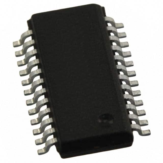
Infineon Technologies TLE8080EMXUMA1
- Part No.:
- TLE8080EMXUMA1
- Manufacturer:
- Infineon Technologies
- Category:
- Power Management - Specialized
- Package:
- 24-LSSOP (0.154", 3.90mm Width) Exposed Pad
- Datasheet:
-
 TLE8080EMXUMA1.pdf
- Description:
- ENGINECONTR
- Quantity:
- Payment:

- Shipping:

Inventory:2,258
Please send an inquiry. Send us your inquiry, and we will respond immediately.
Product details
Overview
TLE8080EMXUMA1 from Infineon is an AEC-qualified engine management IC for small-displacement internal combustion engines, integrating a 5 V ±2% / 250 mA regulator, ISO 9141 K-line transceiver, SPI interface, configurable variable reluctance sensor (VRS) front-end, and five protected low-side drivers - including two 2.6 A inductive load switches, two 350 mA inductive load switches, and one 3 A resistive load switch. It serves as the core power and communication hub in one-cylinder motorcycle ECU designs.
For engineers reviewing the TLE8080EMXUMA1 datasheet, TLE8080EMXUMA1 pinout, TLE8080EMXUMA1 application, or TLE8080EMXUMA1 equivalent, key selection criteria include its integrated K-line compliance, dual-threshold reset with glitch immunity, VRS input sensitivity tuning, channel-specific diagnosis (open-load/short-to-GND), and PG-SSOP24 thermal performance under 150°C junction conditions.
Technical Context
The TLE8080EMXUMA1 implements Smart Power Technology with embedded protection logic across all five output stages: overtemperature shutdown, current limiting, and off-state diagnostics per channel. Its VRS interface supports adjustable gain and hysteresis for crank/cam position sensing, while the K-line transceiver meets ISO 9141-2 physical layer timing and voltage thresholds.
Reset supervision uses a dual-threshold comparator (VRT = 4.55 V rising, 4.35 V falling) with programmable delay (tRD = 10 ms typ.) and glitch rejection (tRR = 10 µs). The 5 V regulator employs a charge-pump-assisted LDO architecture enabling stable operation down to 470 nF ceramic output capacitance at full 250 mA load.
Key Specifications
| Parameter | Value and Actual Design Meaning |
|---|---|
| Supply Input Range | VS = 6–40 V: Enables direct battery connection without external pre-regulation in 12 V automotive systems. |
| 5 V Regulator Output | V5DD = 5.0 V ±2%, 250 mA max: Powers MCU, sensors, and logic; stable with ≥470 nF ceramic cap. |
| Low-Side Driver Channels | 5 total: 2×2.6 A (inductive), 2×350 mA (inductive), 1×3 A (resistive); each with OT/OC protection & off-diagnosis. |
| K-line Compliance | ISO 9141-2: Supports bidirectional diagnostic communication via KIO/TX/RX pins at 10.4 kbaud. |
| VRS Interface | Configurable gain/hysteresis on VR_IN1/VR_IN2; differential input with VR_OUT for signal conditioning. |
| Reset Behavior | NRO open-drain output; active-low reset with 4.55 V/4.35 V hysteresis and 10 ms delay after power-up. |
| Operating Junction Temp | Tj = −40 °C to +150 °C: Validated for under-hood motorcycle ECU environments. |
Pinout & Package
Package: PG-SSOP24 (Plastic Small Outline Package, 24-pin, exposed thermal pad). Pin pitch: 0.65 mm; body size: 7.2 × 5.3 mm; thermal pad must be externally connected to PGND.
| Pin/Terminal | Circuit Role | Design Meaning |
|---|---|---|
| KIO | K-line bus I/O | Bidirectional ISO 9141 physical layer interface; connects directly to vehicle diagnostic line. |
| VS | Main supply input | 6–40 V battery input; requires local 100 nF ceramic decoupling to AGND at IC pin. |
| OUT1–OUT5 | Low-side driver outputs | Five independent NMOS outputs: OUT1/OUT2 = 2.6 A; OUT3/OUT4 = 350 mA; OUT5 = 3 A. |
| IN1, IN3 | Digital control inputs | Logic-level enable inputs for OUT1/OUT3; internal pull-down ensures safe default OFF state. |
| VR_IN1, VR_IN2 | VRS differential input | High-impedance inputs for magnetic sensor signals; support adjustable gain and offset compensation. |
| VR_OUT | VRS conditioned output | Amplified/filtered VR signal output for MCU ADC or comparator input. |
| SCLK, SI, SO, CSN | SPI interface | Full-duplex 4-wire SPI (mode 0, CPOL=0, CPHA=0); SO high-impedance when CSN high. |
| NRO | Reset output | Open-drain active-low reset signal; drives external MCU reset pin with 10 ms delay and glitch immunity. |
| WD_DIS | Watchdog disable | Active-high input; disables watchdog timer if held high during startup or runtime. |
| AGND / PGND | Analog & power ground | Separate AGND (logic reference) and PGND (power return); internally connected but require separate PCB routing. |
Key Features
| Feature | Design Value |
|---|---|
| Integrated 5 V regulator | ±2% accuracy at 250 mA with charge-pump assist enables low-drop operation and eliminates external LDO. |
| Per-channel fault diagnosis | Each low-side driver reports open-load, short-to-GND, and overtemperature status via SPI-accessible registers. |
| Configurable VRS front-end | Adjustable gain and hysteresis on VR_IN1/VR_IN2 allow optimization for different sensor air gaps and speeds. |
| K-line physical layer | Fully compliant ISO 9141-2 transceiver with TX/RX/KIO pins eliminates need for external LIN/K-line interface IC. |
| AEC-Q100 qualification | Qualified to Grade 1 (−40 °C to +125 °C ambient) with extended validation to 150 °C junction temperature. |
Applications
| Motorcycle ECU | Small Engine Diagnostic Tool |
|---|---|
|
Use Scenario: Real-time control of fuel injection, ignition timing, and idle speed in single-cylinder scooter/moped engines. IC Role / Device Role / Timing Role: Central power manager and actuator driver; synchronizes spark/fuel events using VRS-triggered timing windows. Use Value: Reduces BOM count by integrating 5 V regulation, K-line diagnostics, and five protected drivers in one PG-SSOP24 package. |
Use Scenario: Portable handheld tool for reading fault codes and live sensor data from lawnmowers, generators, and ATVs. IC Role / Device Role / Timing Role: K-line protocol translator and VRS signal conditioner; bridges legacy engine ECUs to USB/Bluetooth host. Use Value: Enables ISO 9141 communication without external transceiver and supports wide-range VR sensor inputs (20 mV–2 V peak). |
| Aftermarket Ignition Module | Electric Start Control Unit |
|
Use Scenario: Retrofit electronic ignition system replacing mechanical breaker points in vintage motorcycles and go-karts. IC Role / Device Role / Timing Role: Low-latency VRS-to-spark timing generator with programmable dwell control via SPI. Use Value: Delivers precise spark advance curves using internal VRS edge detection and configurable output dead-time. |
Use Scenario: Starter motor engagement logic with battery voltage monitoring and cranking current limiting. IC Role / Device Role / Timing Role: High-current (3 A) low-side switch (OUT5) with overcurrent shutdown and undervoltage lockout. Use Value: Prevents starter damage during low-battery cranking by disabling OUT5 when V5DD drops below 4.35 V. |
Equivalent & Alternatives
The following parts are listed as comparable options for similar engine management applications.
| Alternative Part | Technical Difference | Application Difference | Selection Advice |
|---|---|---|---|
| TLE8080-2EM | V5DD reset threshold = 4.45 V (rising), power-on reset delay = 20 ms (vs. 10 ms in TLE8080EMXUMA1) | Used where longer reset hold time is required for slower microcontrollers or complex boot sequences. | Select only if system timing analysis confirms need for extended tRD; otherwise, TLE8080EMXUMA1 offers tighter reset precision. |
| TLE8080-3EM | V5DD reset threshold = 4.45 V (rising), identical tRD = 10 ms; differs only in reset threshold vs. main version | Targeted at designs requiring marginally higher reset release voltage while retaining same timing behavior. | Choose when V5DD stability near 4.45 V is critical; verify compatibility with MCU reset spec before substitution. |
Compared with TLE8080-2EM and TLE8080-3EM, the TLE8080EMXUMA1 provides the tightest reset hysteresis (4.55 V / 4.35 V) and shortest guaranteed reset delay (10 ms), making it optimal for fast-booting MCUs and thermally constrained ECU layouts where timing predictability is essential.
Availability
TLE8080EMXUMA1 is available at Aetrix Electronics and suitable for motorcycle ECU design, small-engine diagnostic tools, and aftermarket ignition modules requiring stable component supply, AEC-Q100 compliance, and integrated K-line/VRS functionality.
Supply support for TLE8080EMXUMA1 includes scheduled delivery planning, volume procurement assistance, BOM continuity management, traceable sourcing, and lifecycle availability coordination for OEM customers, industrial embedded developers, connected-device designers, and electronics production programs.
Manufacturer
Infineon Technologies is a German semiconductor manufacturer specializing in power management, automotive ICs, and industrial control solutions, with global R&D and manufacturing infrastructure.
The TLE8080EMXUMA1 belongs to Infineon's Smart Power family, designed specifically for cost-sensitive, thermally demanding engine control units in 1-cylinder gasoline and diesel applications.
FAQ
What is the maximum continuous current rating for OUT5?
OUT5 is rated for 3 A continuous DC current into resistive loads, with built-in overtemperature and overcurrent protection that disables the channel if junction temperature exceeds 165 °C or current exceeds 4.5 A peak for >100 µs. It is not rated for inductive loads - those are assigned to OUT1–OUT4.
Can the VRS interface accept signals from both passive and active VR sensors?
Yes - the VRS interface supports passive variable reluctance sensors (e.g., crankshaft position sensors) via differential AC-coupled input on VR_IN1/VR_IN2, and also accommodates active Hall-effect or magneto-resistive sensors through configurable bias and gain settings accessible via SPI registers.
Is the K-line transceiver fully compliant with ISO 9141-2 without external components?
Yes - the internal K-line circuitry meets all ISO 9141-2 requirements for dominant/recessive voltage levels, slew rate, and bus arbitration timing. Only external 120 Ω termination resistor and optional ESD protection diodes are recommended; no level-shifting or driver ICs are needed.
How does the watchdog function interact with the WD_DIS pin?
The watchdog timer resets the device if not refreshed within ~1.6 s. Holding WD_DIS high (≥2.0 V) disables the watchdog entirely - both timeout detection and reset generation - allowing use in systems where software-based supervision is handled externally or not required.
TLE8080EMXUMA1 Specifications
- Product attributes
- Attribute value
- Manufacturer:
- Infineon Technologies
- Series:
- -
- Package/Case:
- 24-LSSOP (0.154", 3.90mm Width) Exposed Pad
- Packaging:
- Tape & Reel (TR)
- Product Status:
- Active
- Applications:
- Small Engine
- Current - Supply:
- -
- Voltage - Supply:
- 6V ~ 18V
- Operating Temperature:
- -40°C ~ 150°C
- Grade:
- Automotive
- Qualification:
- -
- Mounting Type:
- Surface Mount
- Supplier Device Package:
- PG-SSOP-24
TLE8080EMXUMA1 FAQ
1.How can I place an order for TLE8080EMXUMA1 through Aetrix?
Please submit a Request for Quotation (RFQ) for TLE8080EMXUMA1 on Aetrix. Our sales agent will provide a competitive quotation and guide you through the order confirmation once you accept the terms.
2.Are the price and stock information for TLE8080EMXUMA1 reliable?
The price and inventory of TLE8080EMXUMA1 are updated periodically and may fluctuate due to market conditions. Stock and pricing data are typically refreshed every 24 hours. Quotation validity for TLE8080EMXUMA1 is usually 5 days.
3.What payment methods are accepted for TLE8080EMXUMA1?
We accept Wire Transfer, PayPal, Credit Card, Western Union, MoneyGram, and Escrow for TLE8080EMXUMA1 transactions.
Note: Certain payment methods may incur a processing fee.
4.How is shipping managed for TLE8080EMXUMA1?
TLE8080EMXUMA1 orders can be shipped via leading logistics carriers, including DHL, UPS, FedEx, TNT, or Registered Mail.
Once your TLE8080EMXUMA1 order is processed, you will receive an email with the shipment details and tracking number.
Note: Tracking information may take up to 24 hours to appear. Express delivery typically takes 3–5 business days.
5.How can I obtain technical support or documentation for TLE8080EMXUMA1?
For technical support, including TLE8080EMXUMA1 datasheets, pinout diagrams, or application guidance, please contact our engineering support team. They can provide detailed documentation and assistance for your TLE8080EMXUMA1 requirements.
6.How does Aetrix verify that TLE8080EMXUMA1 is sourced from the original manufacturer or authorized distributors?
All TLE8080EMXUMA1 products on Aetrix are procured from qualified distributors and authorized channels. Our dedicated quality assurance team conducts strict verification, including traceability checks and, if necessary, third-party testing. This ensures that TLE8080EMXUMA1 meets industry standards.
7.What is the process for return or replacement of TLE8080EMXUMA1?
All TLE8080EMXUMA1 units undergo pre-shipment inspection (PSI). If there is an issue with TLE8080EMXUMA1, returns or replacements are accepted under the following conditions:
1.Quantity discrepancies, incorrect items, or visible external defects (such as breakage or corrosion), acknowledged by Aetrix.
2.The issue is reported within 90 days of delivery.
3.The TLE8080EMXUMA1 part is unused and in its original packaging.
Return procedure for TLE8080EMXUMA1:
1.Submit a request within 90 days.
2.Obtain a Return Material Authorization (RMA) from Aetrix.
TLE8080EMXUMA1 Tags

-
TPS2511DGNR
Texas Instruments

-
UTC2000/MG
Microchip Technology

-
TUSB320HAIRWBR
Texas Instruments

-
TPS61252DSGR
Texas Instruments

-
PI5USB30216CXUAEX
Diodes Incorporated

-
SN6501DBVR
Texas Instruments

-
CYPD3177-24LQXQT
Infineon Technologies
-
SN6501QDBVRQ1
Texas Instruments

-
STUSB1600AQTR
STMicroelectronics

-
SN6505BDBVR
Texas Instruments
-
SN6501DBVT
Texas Instruments

-
TPS65150PWPR
Texas Instruments
Tech Hub

Guide to electronic component obsolescence covering EOL risk, PCN/PDN notices, last-time buy planning, replacement options, form-fit-function validation, counterfeit risk and BOM lifecycle management.

18650 battery guide covering lithium-ion cell basics, 3.6V/3.7V voltage, 4.2V charging, mAh and Wh capacity, protected cells, chargers, BMS, series-parallel packs, holders, welding and sourcing checks.…

Hall effect sensor guide covering working principle, linear and digital sensors, Arduino circuits, current sensing, speed detection, automotive applications, A3144 examples, signal filtering and datash…

Product Change Notification guide for electronic components, covering PCN meaning, PCN vs PDN/EOL, common change types, risk levels, form-fit-function review, engineering validation, BOM control, LTB/L…

A practical guide to blend door actuators, covering HVAC function, symptoms, location, AC and heater issues, reset and calibration, replacement cost, electrical diagnosis, compatibility checks, and rep…

Engineering guide to Raspberry Pi alternatives, covering chip-level differences, Orange Pi, ROCK, Jetson, Banana Pi, NanoPi, Compute Module, Pico, GPIO, camera, HAT compatibility, and replacement risks…

Engineering guide to dynamic load response testing for high-current buck converters, covering load step setup, slew rate, Vcore undershoot, overshoot, recovery time, probe location, output capacitors a…

Engineering guide to output capacitor selection for ASIC Vcore rails, covering bulk capacitors, polymer capacitors, MLCC decoupling, DC bias, ESR, ESL, placement, transient response and substitution ri…

Engineering guide to high-current ASIC Vcore rails, covering 12-phase buck architecture, PMBus control, dynamic load testing, output capacitor networks, smart power stage selection, thermal design and …

Voltage regulator guide covering linear, LDO, 7805, Zener, adjustable, buck, VRM and alternator regulators, with design checks, testing methods, troubleshooting and datasheet-based selection.


