
 My Inquiry
 My Account


Infineon Technologies TLE9254VLCXUMA1
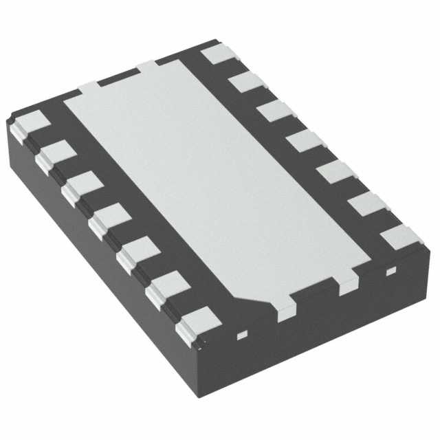
- Part No.:
- TLE9254VLCXUMA1
- Manufacturer:
- Infineon Technologies
- Category:
- Drivers, Receivers, Transceivers
- Package:
- 14-TDFN Exposed Pad
- Datasheet:
-
 TLE9254VLCXUMA1.pdf
- Description:
- IC TRANSCEIVER HALF 2/2 TSON-14
- Quantity:
- Payment:

- Shipping:

Inventory:1,288
Please send an inquiry. Send us your inquiry, and we will respond immediately.
Product details
Overview
TLE9254VLCXUMA1 from Infineon is a high-speed dual-channel CAN FD transceiver compliant with ISO 11898-2:2016, designed for automotive HS CAN networks. It supports data rates up to 5 Mbit/s, features bus wake-up pattern detection, achieves <10 µA quiescent current per channel in stand-by mode, and operates across extended VCC (4.5–6.0 V) and VIO (3.0–6.0 V) supply ranges. It is deployed in body control modules and gateway systems requiring robust ESD immunity and low EME.
For engineers reviewing the TLE9254VLCXUMA1 datasheet, TLE9254VLCXUMA1 pinout, TLE9254VLCXUMA1 application, or TLE9254VLCXUMA1 equivalent, key selection criteria include dual-channel CAN FD timing symmetry, bus wake-up sensitivity, stand-by current consumption, and AEC-Q100 qualification for automotive deployment.
Technical Context
The TLE9254VLCXUMA1 integrates two independent high-speed CAN FD transceivers sharing a common VIO rail and separate STB/TxD/RxD/CANH/CANL terminals per channel. Its transmitter delivers <±1% differential output symmetry at 5 Mbit/s, while the receiver employs dual-path architecture-normal-mode and low-power wake-up path-with programmable wake-up pattern filtering.
It implements fail-safe functions including TxD timeout (programmable via external RC), overtemperature shutdown (>150°C), undervoltage lockout on VCC and VIO, and short-circuit protection to battery, ground, and VCC. The device supports voltage-adaptive logic I/O via VIO and maintains passive bus behavior during power-off.
Key Specifications
| Parameter | Value and Actual Design Meaning |
|---|---|
| CAN FD Data Rate | Up to 5 Mbit/s - enables high-bandwidth firmware updates and sensor fusion in modern ECUs. |
| Stand-by Current (per channel) | <10 µA typical - extends battery life in always-on automotive modules like gateways and BCMs. |
| Common Mode Range | ±40 V - ensures reliable operation under severe electromagnetic interference in vehicle harnesses. |
| ESD Robustness (CANH/CANL) | ±10 kV HBM - eliminates need for external TVS diodes in most automotive PCB layouts. |
| VIO Supply Range | 3.0–6.0 V - allows direct interfacing with both 3.3 V and 5 V microcontrollers without level shifters. |
| Operating Junction Temp | -40°C to +150°C - qualified for under-hood and transmission-control applications per AEC-Q100 Grade 0. |
| EME Performance | No external common-mode choke required - reduces BOM cost and board space in compact modules. |
Pinout & Package
The TLE9254VLCXUMA1 is housed in a PG-TSON-14 (leadless, thermally enhanced) package with exposed thermal pad, RoHS-compliant and halogen-free, supporting AOI solder-joint inspection.
| Pin/Terminal | Circuit Role | Design Meaning |
|---|---|---|
| TxD1 / TxD2 | Transmit Data Input | CMOS-level input with internal pull-up to VCC; dominant state = low; controls CANH/CANL driver state. |
| RxD1 / RxD2 | Receive Data Output | CMOS-level open-drain output; dominant = low; indicates bus state; doubles as wake-up indicator in stand-by. |
| CANH1 / CANH2 | CAN Bus High I/O | Differential high-side bus terminal; outputs 2.75–3.75 V in recessive state; drives dominant to ~3.5 V above CANL. |
| CANL1 / CANL2 | CAN Bus Low I/O | Differential low-side bus terminal; outputs 1.25–2.25 V in recessive state; driven to ~1.5 V below CANH in dominant. |
| STB1 / STB2 | Stand-by Control Input | Active-high enable; internal pull-up to VCC; asserts stand-by mode when high, reducing current to <10 µA per channel. |
| VCC | Transmitter Supply | 4.5–6.0 V analog supply for CAN drivers; requires 100 nF decoupling to GND; can be powered down in stand-by. |
| VIO | Digital Interface Supply | 3.0–6.0 V supply for logic interface; sets TxD/RxD voltage thresholds; remains active during stand-by. |
| GND1 / GND2 | Analog Ground Returns | Separate ground pins per channel; must be connected to same PCB ground plane to minimize ground bounce. |
| PAD | Thermal Pad | Exposed copper pad on bottom; must be soldered to PCB thermal plane (GND-connected) for thermal management. |
Key Features
| Feature | Design Value |
|---|---|
| Dual independent CAN FD channels | Enables simultaneous communication on two isolated HS CAN buses (e.g., powertrain + body domain) without MCU resource contention. |
| Bus wake-up pattern detection | Hardware-filtered wake-up recognition on CANH/CANL without CPU involvement, reducing system latency and power. |
| Low EME emission profile | Meets CISPR 25 Class 5 limits without external common-mode chokes, simplifying layout and lowering BOM cost. |
| TxD timeout protection | Prevents bus lock-up by disabling transmitter after configurable timeout (via external RC), protecting network integrity. |
| AEC-Q100 Grade 0 qualification | Validated for operation from -40°C to +150°C junction temperature, meeting requirements for engine bay and transmission control. |
Applications
| Gateway Modules | Body Control Modules (BCMs) |
|---|---|
|
Use Scenario: Aggregating messages between powertrain, chassis, and infotainment CAN FD networks in modern vehicle architectures. IC Role / Device Role / Timing Role: Dual-channel physical layer interface enabling concurrent high-speed bridging with independent wake-up capability per bus. Use Value: Reduces gateway MCU load and latency while maintaining <10 µA sleep current per channel for always-on network monitoring. |
Use Scenario: Centralized control of lighting, door locks, window lifts, and HVAC in electric and hybrid vehicles. IC Role / Device Role / Timing Role: HS CAN FD transceiver interfacing with 3.3 V or 5 V microcontrollers via VIO, supporting firmware OTA updates at 5 Mbit/s. Use Value: Eliminates need for external level shifters and ESD protection, shrinking PCB area and improving EMC robustness. |
| Electric Power Steering (EPS) | Battery Management Systems (BMS) |
|
Use Scenario: Real-time torque and position feedback loop between EPS ECU and motor controller over HS CAN FD. IC Role / Device Role / Timing Role: Fault-tolerant CAN physical layer with overtemperature shutdown and short-circuit protection to battery/ground/VCC. Use Value: Ensures functional safety compliance (ISO 26262 ASIL-B capable) through integrated fail-safe mechanisms and AEC-Q100 validation. |
Use Scenario: Cell voltage, temperature, and SOC reporting from battery packs to vehicle controller via isolated CAN FD link. IC Role / Device Role / Timing Role: High-common-mode-range transceiver (±40 V) tolerant of pack-level ground offsets and transient noise in high-voltage systems. Use Value: Maintains communication integrity during load dump (ISO 7637-2 Pulse 5a) and jump-start events without external protection. |
Equivalent & Alternatives
The following parts are listed as comparable options for similar dual-channel CAN FD transceiver applications.
| Alternative Part | Technical Difference | Application Difference | Selection Advice |
|---|---|---|---|
| NXP TJA1044GT/3 | Single-channel CAN FD transceiver; no dual-channel integration; lower ESD rating (±8 kV HBM on CANH/L). | Requires two devices for dual-bus operation; lacks integrated bus wake-up pattern detection logic. | Select when only one CAN FD bus is needed and cost-per-channel is prioritized over integration. |
| ST TLE6250G | Legacy high-speed CAN (non-FD); max 1 Mbit/s; no VIO pin; fixed 5 V logic interface; no stand-by wake-up pattern support. | Not suitable for CAN FD data frames or 3.3 V microcontrollers; lacks low-power wake-up capability. | Select only for legacy CAN 2.0B designs where FD bandwidth and ultra-low stand-by current are not required. |
Compared with TJA1044GT/3 and TLE6250G, the TLE9254VLCXUMA1 uniquely delivers dual-channel CAN FD at 5 Mbit/s with hardware wake-up pattern detection, sub-10 µA stand-by current, and flexible VIO-based logic interfacing - making it optimal for next-generation automotive domain controllers.
Availability
TLE9254VLCXUMA1 is available at Aetrix Electronics and suitable for gateway modules, body control units, and battery management systems requiring stable component supply, AEC-Q100 qualification, and long-term automotive lifecycle support.
Supply support for TLE9254VLCXUMA1 includes scheduled delivery planning, volume procurement assistance, BOM continuity management, traceable sourcing, and lifecycle availability coordination for OEM customers, industrial embedded developers, connected-device designers, and electronics production programs.
Manufacturer
Infineon Technologies is a German semiconductor manufacturer specializing in power management, automotive ICs, and security solutions, with leadership in automotive-grade analog and mixed-signal products.
The TLE9254VLCXUMA1 belongs to Infineon's automotive CAN transceiver product line, engineered specifically for high-reliability, low-power, dual-bus HS CAN FD communication in demanding automotive environments.
FAQ
What is the maximum supported CAN FD data rate for TLE9254VLCXUMA1?
The TLE9254VLCXUMA1 supports CAN FD data frames up to 5 Mbit/s, enabled by its high transmitter symmetry (<±1%) and optimized receiver delay matching. This performance is validated per ISO 11898-2:2016 and confirmed in Infineon's characterization reports across temperature and voltage ranges.
Does TLE9254VLCXUMA1 require an external common-mode choke?
No. Due to its very low electromagnetic emission (EME) profile across 1–100 MHz, the TLE9254VLCXUMA1 meets CISPR 25 Class 5 limits without an external common-mode choke - a design advantage verified in Infineon's EMC test reports and application notes.
How does the bus wake-up pattern function operate?
The wake-up pattern detector monitors CANH/CANL for standardized dominant-recessive sequences (e.g., 0x55 or 0xAA). Upon match, it asserts RxD low to signal wake-up while remaining in stand-by; no MCU intervention is required until full channel activation.
Is TLE9254VLCXUMA1 compatible with both 3.3 V and 5 V microcontrollers?
Yes. Its VIO pin accepts 3.0–6.0 V, allowing direct interface with 3.3 V or 5 V MCUs. Logic thresholds scale with VIO, ensuring correct TxD sampling and RxD output levels without external level-shifting circuitry.
TLE9254VLCXUMA1 Specifications
- Product attributes
- Attribute value
- Manufacturer:
- Infineon Technologies
- Series:
- -
- Package/Case:
- 14-TDFN Exposed Pad
- Packaging:
- Tape & Reel (TR)
- Product Status:
- Obsolete
- Type:
- Transceiver
- Protocol:
- CANbus
- Number of Drivers/Receivers:
- 2/2
- Duplex:
- Half
- Receiver Hysteresis:
- 50 mV
- Data Rate:
- 5Mbps
- Voltage - Supply:
- 4.5V ~ 5.5V
- Operating Temperature:
- -40°C ~ 150°C (TJ)
- Grade:
- Automotive
- Qualification:
- AEC-Q100
- Mounting Type:
- Surface Mount, Wettable Flank
- Supplier Device Package:
- PG-TSON-14-3
TLE9254VLCXUMA1 FAQ
1.How can I place an order for TLE9254VLCXUMA1 through Aetrix?
Please submit a Request for Quotation (RFQ) for TLE9254VLCXUMA1 on Aetrix. Our sales agent will provide a competitive quotation and guide you through the order confirmation once you accept the terms.
2.Are the price and stock information for TLE9254VLCXUMA1 reliable?
The price and inventory of TLE9254VLCXUMA1 are updated periodically and may fluctuate due to market conditions. Stock and pricing data are typically refreshed every 24 hours. Quotation validity for TLE9254VLCXUMA1 is usually 5 days.
3.What payment methods are accepted for TLE9254VLCXUMA1?
We accept Wire Transfer, PayPal, Credit Card, Western Union, MoneyGram, and Escrow for TLE9254VLCXUMA1 transactions.
Note: Certain payment methods may incur a processing fee.
4.How is shipping managed for TLE9254VLCXUMA1?
TLE9254VLCXUMA1 orders can be shipped via leading logistics carriers, including DHL, UPS, FedEx, TNT, or Registered Mail.
Once your TLE9254VLCXUMA1 order is processed, you will receive an email with the shipment details and tracking number.
Note: Tracking information may take up to 24 hours to appear. Express delivery typically takes 3–5 business days.
5.How can I obtain technical support or documentation for TLE9254VLCXUMA1?
For technical support, including TLE9254VLCXUMA1 datasheets, pinout diagrams, or application guidance, please contact our engineering support team. They can provide detailed documentation and assistance for your TLE9254VLCXUMA1 requirements.
6.How does Aetrix verify that TLE9254VLCXUMA1 is sourced from the original manufacturer or authorized distributors?
All TLE9254VLCXUMA1 products on Aetrix are procured from qualified distributors and authorized channels. Our dedicated quality assurance team conducts strict verification, including traceability checks and, if necessary, third-party testing. This ensures that TLE9254VLCXUMA1 meets industry standards.
7.What is the process for return or replacement of TLE9254VLCXUMA1?
All TLE9254VLCXUMA1 units undergo pre-shipment inspection (PSI). If there is an issue with TLE9254VLCXUMA1, returns or replacements are accepted under the following conditions:
1.Quantity discrepancies, incorrect items, or visible external defects (such as breakage or corrosion), acknowledged by Aetrix.
2.The issue is reported within 90 days of delivery.
3.The TLE9254VLCXUMA1 part is unused and in its original packaging.
Return procedure for TLE9254VLCXUMA1:
1.Submit a request within 90 days.
2.Obtain a Return Material Authorization (RMA) from Aetrix.
TLE9254VLCXUMA1 Tags

-
ATA6561-GAQW-N
Microchip Technology
-
ATA6561-GBQW-N
Microchip Technology

-
AM26LS32ACDR
Texas Instruments

-
SP485CN-L/TR
MaxLinear, Inc.
-
SP485EN-L/TR
MaxLinear, Inc.
-
SP485EEN-L/TR
MaxLinear, Inc.
-
SP485ECN-L/TR
MaxLinear, Inc.
-
THVD1400DR
Texas Instruments
-
AM26C31IDR
Texas Instruments

-
TLIN1021ADRQ1
Texas Instruments
-
MAX232IDR
Texas Instruments
-
AM26C32IDR
Texas Instruments
Tech Hub

LDO regulator guide covering low dropout voltage, power dissipation, thermal design, PSRR, output noise, capacitor stability, adjustable LDO circuits, LDO vs buck converter and datasheet selection chec…

Conditional Access Module guide covering CAM meaning, CI/CI+ interface, smart card authorization, DVB security workflow, TV and set-top box compatibility, internal electronics, ESD protection, connecto…

Guide to electronic component obsolescence covering EOL risk, PCN/PDN notices, last-time buy planning, replacement options, form-fit-function validation, counterfeit risk and BOM lifecycle management.

18650 battery guide covering lithium-ion cell basics, 3.6V/3.7V voltage, 4.2V charging, mAh and Wh capacity, protected cells, chargers, BMS, series-parallel packs, holders, welding and sourcing checks.…

Hall effect sensor guide covering working principle, linear and digital sensors, Arduino circuits, current sensing, speed detection, automotive applications, A3144 examples, signal filtering and datash…

Product Change Notification guide for electronic components, covering PCN meaning, PCN vs PDN/EOL, common change types, risk levels, form-fit-function review, engineering validation, BOM control, LTB/L…

A practical guide to blend door actuators, covering HVAC function, symptoms, location, AC and heater issues, reset and calibration, replacement cost, electrical diagnosis, compatibility checks, and rep…

Engineering guide to Raspberry Pi alternatives, covering chip-level differences, Orange Pi, ROCK, Jetson, Banana Pi, NanoPi, Compute Module, Pico, GPIO, camera, HAT compatibility, and replacement risks…

Engineering guide to dynamic load response testing for high-current buck converters, covering load step setup, slew rate, Vcore undershoot, overshoot, recovery time, probe location, output capacitors a…

Engineering guide to output capacitor selection for ASIC Vcore rails, covering bulk capacitors, polymer capacitors, MLCC decoupling, DC bias, ESR, ESL, placement, transient response and substitution ri…


