Send an Inquiry

To receive a quote for your project, please fill in the following information, and we’ll get back to you promptly.

Name*
Company*
Email Address*
Phone/WhatsApp
Part Number*
Quantity*
Message
Submit Inventory List

Please fill in the following information, and we’ll get back to you promptly.

Name*
Company*
Email Address*
Phone/WhatsApp
Upload My List
Message

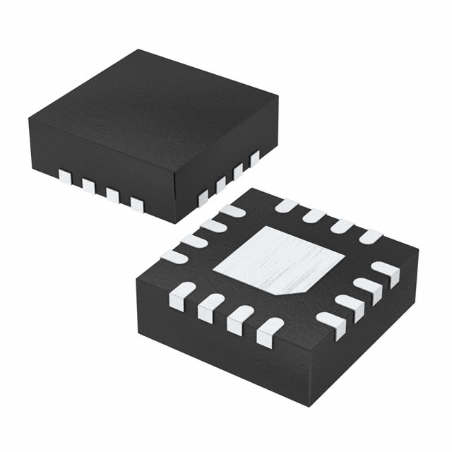
Silicon Labs TS1107-20ITQ1633T

Part No.:
TS1107-20ITQ1633T
Manufacturer:
Silicon Labs
Category:
Instrumentation, Op Amps, Buffer Amps
Package:
16-WFQFN Exposed Pad
Datasheet:
AetrixTS1107-20ITQ1633T.pdf
Description:
IC CURRENT SENSE 1 CIRCUIT 16QFN
Quantity:
Payment:
Payment
Shipping:
Shipping

Inventory:500

Please send an inquiry. Send us your inquiry, and we will respond immediately.

Part Number
Quantity*
Price
Name*
Company
Email*
Comments

Product details

Overview

TS1107-20ITQ1633T from Silicon Labs is a high-side bidirectional current-sense amplifier with internal latching current-limit comparator, 20 V/V gain, 150 µV max input offset voltage, ±1% max gain error, and 2 V to 27 V input common-mode range - used for overcurrent detection and load monitoring in battery-powered systems.

For engineers reviewing the TS1107-20ITQ1633T datasheet, TS1107-20ITQ1633T pinout, TS1107-20ITQ1633T application, or TS1107-20ITQ1633T equivalent, key selection considerations include bidirectional sensing capability, programmable current-limit threshold via external reference, latch-reset control via CLATCH, low quiescent supply current (1.15 µA typ), and compatibility with Kelvin-sense PCB layouts for precision measurement.

Technical Context

The TS1107-20ITQ1633T implements a fully differential, high-side current-sense amplifier with dual PMOS input stage enabling true bidirectional operation without dead zone at zero-crossing. Its transimpedance output buffer delivers VOUT = VBIAS ± ILOAD × RSENSE × (ROUT / RGAIN), where RGAIN = 2 kΩ and ROUT = 40 kΩ for 20 V/V gain.

It integrates a latching current-limit comparator with CIN– tied to OUT and CIN+ accepting an external threshold voltage; latch enable requires CLATCH = HIGH, and reset occurs only when CLATCH is strobed or held LOW. Unlike the TS1110, this variant lacks FET gate drive - it provides only current sensing and fault signaling via COUT.

Key Specifications

ParameterValue and Actual Design Meaning
Gain20 V/V - sets output scaling: ±1 mV sense voltage yields ±20 mV output swing, enabling accurate low-current measurement with minimal RSENSE power loss.
Input Offset Voltage±150 µV max - contributes ≤ ±3 mV error at full-scale 20× gain, critical for sub-100 mA current detection accuracy.
Common-Mode Range+2 V to +27 V - supports direct high-side sensing across wide input rails including 12 V, 24 V, and 19 V laptop adapters without level-shifting.
Supply Current1.15 µA typ (IVDD) - enables multi-year battery life in always-on portable monitors and smart chargers.
CMRR130 dB typ - rejects noise from switching regulators and motor drives, preserving signal integrity in noisy industrial environments.
Operating Temp–40 °C to +85 °C - qualified for automotive cabin electronics, industrial PLCs, and outdoor energy storage systems.
Package16-pin TQFN (3 mm × 3 mm) - compact footprint with exposed pad for thermal dissipation and low-inductance ground path.

Pinout & Package

TS1107-20ITQ1633T uses a 16-pin 3 mm × 3 mm TQFN package with exposed thermal pad (EPAD), optimized for low-noise current sensing and PCB thermal management. Pin 1 is marked by a laser-etched circle in the lower-left corner.

Pin/TerminalCircuit RoleDesign Meaning
SIGNDirection indicator outputLogic HIGH when VRS+ > VRS– (positive load current); LOW when reversed - enables bidirectional energy flow monitoring in USB PD and battery protection circuits.
VDDPower supply inputAccepts 1.7–5.25 V; powers internal bias circuitry and buffer - decoupling capacitor required near pin for stability.
VBIASCSA output bias referenceInternally set to 50% of VREF when VREF ≥ 0.9 V; eliminates need for external bias network and reduces component count.
GNDAnalog ground referenceMust connect to low-impedance analog ground plane; EPAD soldered to same plane ensures optimal noise immunity and thermal performance.
CIN–Comparator inverting inputConnected to OUT pin - forms feedback path for current-limit detection; enables threshold comparison against sensed load current.
CIN+Comparator non-inverting inputAccepts external voltage divider or DAC output - sets precise overcurrent trip point independent of supply rail variations.
NC (Pin 7)No connectionNot internally bonded - must remain unconnected to avoid parasitic coupling or ESD risk.
VREFReference activation input≥ 0.9 V enables internal 9.2 MΩ divider to generate VBIAS; grounded to disable - allows flexible bias configuration.
OUTBuffered current-sense outputDelivers amplified, filtered VSENSE with rail-to-rail swing (0.2 V to VDD – 0.2 V) - directly interfaces with ADCs or comparator inputs.
FILTFilter node accessConnects to inverting terminal of transimpedance amplifier - supports external RC filter (e.g., 4 kΩ + 0.47 µF) to suppress high-frequency noise.
RS+High-side sense resistor terminalConnects to power rail side of RSENSE - designed for Kelvin routing to eliminate PCB trace resistance errors.
RS–Low-side sense resistor terminalConnects to load side of RSENSE - for TS1107, load connects directly here; no external MOSFET gate drive capability.
NC (Pin 13)No connectionUnbonded in TS1107 - distinct from TS1110's FET pin; must be left floating per datasheet.
NC (Pin 14)No connectionUnbonded - no internal connection; leave unconnected.
CLATCHLatch enable/reset controlCMOS-compatible input: HIGH enables latch mode; LOW resets COUT after fault - enables manual or microcontroller-driven recovery.
COUTLatched fault outputOpen-drain or push-pull (configurable) output signals persistent overcurrent condition - drives LEDs, interrupts, or system shutdown logic.

Key Features

FeatureDesign Value
Bidirectional current sensingZero-dead-zone SIGN output enables accurate charge/discharge monitoring in battery management without polarity ambiguity.
Internal latching comparatorCOUT remains asserted until CLATCH is actively pulled low - prevents transient faults from causing intermittent load disconnects.
Programmable current limitCIN+ accepts user-defined threshold voltage - supports adaptive trip points for varying load profiles or temperature compensation.
Integrated 50 kHz noise filter2nd-order differential low-pass filter eliminates need for external RC networks - avoids gain/offset errors introduced by discrete filters.
Low-offset, high-CMRR architecture150 µV max VOS and 130 dB CMRR ensure <0.1% error in 12 V systems with 100 kHz switching noise - critical for precision power telemetry.

Applications

Battery Protection CircuitSmart Charger Monitoring

Use Scenario: Real-time monitoring of Li-ion battery pack charge/discharge current during fast charging and protection against overcurrent events.

IC Role / Device Role / Timing Role: High-side current-sense amplifier with latched fault signaling - measures bidirectional current and asserts COUT on violation.

Use Value: Enables compliance with JEITA and IEC 62133 safety standards using single-chip solution with <1.2 µA supply current and Kelvin-sense layout support.

Use Scenario: Accurate current regulation and fault detection in USB-C PD chargers supporting variable voltage/current profiles.

IC Role / Device Role / Timing Role: Bidirectional CSA providing real-time load current feedback to MCU and latched overcurrent interrupt via COUT.

Use Value: Supports ±1% current measurement accuracy across 0–5 A range with 20 V/V gain and 150 µV offset - eliminating need for calibration in production.

Industrial Power Rail MonitorPortable Medical Device Power Management

Use Scenario: Continuous supervision of 24 V DC power distribution in PLC I/O modules to detect short-circuits and degraded wiring.

IC Role / Device Role / Timing Role: High-common-mode current sensor interfacing to isolated ADC and fault controller - operates up to +27 V CM range.

Use Value: Delivers stable 130 dB CMRR and 428 µs system delay for rapid fault response while rejecting noise from adjacent motor drivers and solenoids.

Use Scenario: Low-power current monitoring in handheld ultrasound or glucose meters requiring multi-year battery life and medical-grade accuracy.

IC Role / Device Role / Timing Role: Ultra-low-quiescent (1.15 µA) bidirectional CSA with latch-reset control - enables always-on current telemetry without compromising runtime.

Use Value: Achieves <0.5% total error over –40 °C to +85 °C using internal VREF divider and matched gain resistors - meets ISO 13485 design validation requirements.

Equivalent & Alternatives

The following parts are listed as comparable options for similar high-side current-sense amplifier applications.

Alternative PartTechnical DifferenceApplication DifferenceSelection Advice
MAX40056ATA+TSingle-direction (high-side only), 100 V/V fixed gain, no SIGN output, 2.7–5.5 V supply, 1.2 µA IQLacks bidirectional sensing and latch reset - suitable only for unidirectional overcurrent cutoff, not energy flow analysis.Select when only positive-current limiting is needed and board space permits larger SOIC-8 package.
INA240A1QDRQ1Automotive-grade (AEC-Q100), 20 V/V gain, 120 V common-mode, 2.6 µA IQ, no latch or SIGN outputHigher voltage rating but no integrated comparator or direction indication - requires external comparator and logic for fault handling.Choose for automotive under-hood applications requiring 125 °C operation and ASIL-B compliance, accepting added external components.

Compared with MAX40056ATA+T and INA240A1QDRQ1, TS1107-20ITQ1633T uniquely combines bidirectional sensing, latched fault signaling, and ultra-low supply current in a 3 mm × 3 mm package - making it optimal for space-constrained, battery-sensitive, and energy-flow-aware designs.

Availability

TS1107-20ITQ1633T is available at Aetrix Electronics and suitable for portable/battery-powered systems, smart chargers, and industrial controls requiring stable component supply, long-term lifecycle support, and consistent parametric performance across production batches.

Supply support for TS1107-20ITQ1633T includes scheduled delivery planning, volume procurement assistance, BOM continuity management, traceable sourcing, and lifecycle availability coordination for OEM customers, industrial embedded developers, connected-device designers, and electronics production programs.

Manufacturer

Silicon Labs is a fabless semiconductor company specializing in precision analog, timing, and mixed-signal ICs for energy-efficient, connected systems.

The TS1107 series belongs to Silicon Labs' electronic circuit protection product line, engineered specifically for high-accuracy, low-power current monitoring and overcurrent response in portable, industrial, and battery-management applications.

FAQ

What is the function of the FILT pin on the TS1107-20ITQ1633T?

The FILT pin on the TS1107-20ITQ1633T provides access to the inverting terminal of the transimpedance amplifier, allowing designers to add an external RC filter (e.g., 4 kΩ + 0.47 µF to GND) to reduce high-frequency noise at the OUT pin. This internal node enables effective 50 kHz differential low-pass filtering without degrading gain accuracy or introducing offset errors associated with external passive filters - a key advantage over discrete solutions.

Does the TS1107-20ITQ1633T support bidirectional current sensing, and how is direction indicated?

Yes, the TS1107-20ITQ1633T supports true bidirectional current sensing with no dead zone at zero-crossing. Direction is indicated by the SIGN output: logic HIGH when VRS+ > VRS– (positive current flow), and logic LOW when VRS– > VRS+ (reverse current). This feature is implemented via dual PMOS input stages that alternately conduct based on sense voltage polarity - enabling precise energy flow tracking in battery charge/discharge and regenerative braking applications.

Can the TS1107-20ITQ1633T drive an external P-channel MOSFET directly?

No, the TS1107-20ITQ1633T does not include FET gate drive capability. Unlike the TS1110 variant, the TS1107-20ITQ1633T has a no-connect (NC) on Pin 13 and provides only current sensing and latched comparator output (COUT). To implement circuit breaker functionality, an external comparator or microcontroller must interpret COUT and drive the gate of a P-channel MOSFET - whereas the TS1110-20ITQ1633T integrates that FET control logic.

What is the recommended method to set the current-limit threshold for the TS1107-20ITQ1633T?

The current-limit threshold for the TS1107-20ITQ1633T is set by applying a precise voltage to the CIN+ pin, while connecting CIN– to the OUT pin. This configuration compares the amplified sense voltage against the external reference. A resistor divider from VDD or a DAC output can provide the threshold voltage; for example, 750 mV on CIN+ triggers fault detection when |ILOAD × RSENSE| × 20 ≥ 750 mV. The latch remains active until CLATCH is pulled LOW - ensuring reliable fault capture even during brief transients.

How does the VREF pin affect biasing in the TS1107-20ITQ1633T?

The VREF pin on the TS1107-20ITQ1633T activates an internal 9.2 MΩ voltage divider when ≥ 0.9 V is applied, generating VBIAS at exactly 50% of VREF - e.g., 1.0 V on VREF yields 0.5 V on VBIAS. When VREF is grounded, the divider is disabled and VBIAS floats (must be left open). This eliminates external bias resistors and improves accuracy by removing matching and drift errors - a design advantage for stable, low-component-count current-sense front-ends.

TS1107-20ITQ1633T Specifications

Product attributes
Attribute value
Manufacturer:
Silicon Labs
Series:
-
Package/Case:
16-WFQFN Exposed Pad
Packaging:
Tape & Reel (TR)
Product Status:
Obsolete
Amplifier Type:
Current Sense
Number of Circuits:
1
Output Type:
-
Slew Rate:
-
Gain Bandwidth Product:
-
-3db Bandwidth:
-
Current - Input Bias:
300 pA
Voltage - Input Offset:
100 µV
Current - Supply:
1.84µA
Current - Output / Channel:
-
Voltage - Supply Span (Min):
1.7 V
Voltage - Supply Span (Max):
5.25 V
Operating Temperature:
-40°C ~ 85°C
Grade:
-
Qualification:
-
Mounting Type:
Surface Mount
Supplier Device Package:
16-QFN (3x3)

TS1107-20ITQ1633T FAQ

1.How can I place an order for TS1107-20ITQ1633T through Aetrix?

Please submit a Request for Quotation (RFQ) for TS1107-20ITQ1633T on Aetrix. Our sales agent will provide a competitive quotation and guide you through the order confirmation once you accept the terms.

2.Are the price and stock information for TS1107-20ITQ1633T reliable?

The price and inventory of TS1107-20ITQ1633T are updated periodically and may fluctuate due to market conditions. Stock and pricing data are typically refreshed every 24 hours. Quotation validity for TS1107-20ITQ1633T is usually 5 days.

3.What payment methods are accepted for TS1107-20ITQ1633T?

We accept Wire Transfer, PayPal, Credit Card, Western Union, MoneyGram, and Escrow for TS1107-20ITQ1633T transactions.

Note: Certain payment methods may incur a processing fee.

4.How is shipping managed for TS1107-20ITQ1633T?

TS1107-20ITQ1633T orders can be shipped via leading logistics carriers, including DHL, UPS, FedEx, TNT, or Registered Mail.

Once your TS1107-20ITQ1633T order is processed, you will receive an email with the shipment details and tracking number.

Note: Tracking information may take up to 24 hours to appear. Express delivery typically takes 3–5 business days.

5.How can I obtain technical support or documentation for TS1107-20ITQ1633T?

For technical support, including TS1107-20ITQ1633T datasheets, pinout diagrams, or application guidance, please contact our engineering support team. They can provide detailed documentation and assistance for your TS1107-20ITQ1633T requirements.

6.How does Aetrix verify that TS1107-20ITQ1633T is sourced from the original manufacturer or authorized distributors?

All TS1107-20ITQ1633T products on Aetrix are procured from qualified distributors and authorized channels. Our dedicated quality assurance team conducts strict verification, including traceability checks and, if necessary, third-party testing. This ensures that TS1107-20ITQ1633T meets industry standards.

7.What is the process for return or replacement of TS1107-20ITQ1633T?

All TS1107-20ITQ1633T units undergo pre-shipment inspection (PSI). If there is an issue with TS1107-20ITQ1633T, returns or replacements are accepted under the following conditions:

1.Quantity discrepancies, incorrect items, or visible external defects (such as breakage or corrosion), acknowledged by Aetrix.

2.The issue is reported within 90 days of delivery.

3.The TS1107-20ITQ1633T part is unused and in its original packaging.

Return procedure for TS1107-20ITQ1633T:

1.Submit a request within 90 days.

2.Obtain a Return Material Authorization (RMA) from Aetrix.

TS1107-20ITQ1633T Tags

  • TS1107-20ITQ1633T
  • TS1107-20ITQ1633T PDF
  • TS1107-20ITQ1633T Datasheet
  • TS1107-20ITQ1633T Specifications
  • TS1107-20ITQ1633T Images
  • Silicon Labs
  • Silicon Labs TS1107-20ITQ1633T
  • Buy TS1107-20ITQ1633T
  • TS1107-20ITQ1633T Price
  • TS1107-20ITQ1633T Distributor
  • TS1107-20ITQ1633T Supplier
  • TS1107-20ITQ1633T Wholesale
Related Products
LM358DT
LM358DT

STMicroelectronics

LM358DR
LM358DR

Texas Instruments

LM2904DR
LM2904DR

Texas Instruments

LM358ADR
LM358ADR

Texas Instruments

LM2904DGKR
LM2904DGKR

Texas Instruments

LM324DR
LM324DR

Texas Instruments

MCP6006T-E/OT
MCP6006T-E/OT

Microchip Technology

MCP6006UT-E/OT
MCP6006UT-E/OT

Microchip Technology

LM324PWR
LM324PWR

Texas Instruments

LM2902PWR
LM2902PWR

Texas Instruments

LM2902DR
LM2902DR

Texas Instruments

LM358P
LM358P

Texas Instruments

Tech Hub

Search

Search

PRODUCT

PRODUCT

PHONE

PHONE

USER

USER