Send an Inquiry

To receive a quote for your project, please fill in the following information, and we’ll get back to you promptly.

Name*
Company*
Email Address*
Phone/WhatsApp
Part Number*
Quantity*
Message
Submit Inventory List

Please fill in the following information, and we’ll get back to you promptly.

Name*
Company*
Email Address*
Phone/WhatsApp
Upload My List
Message

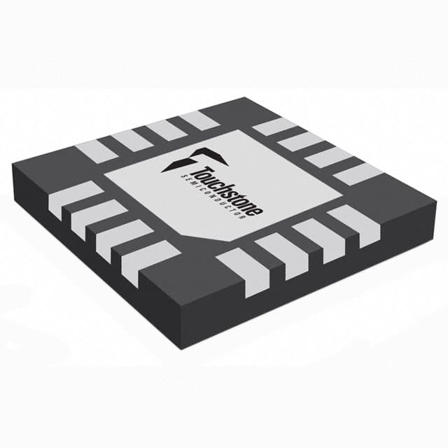
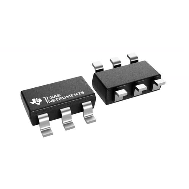
Silicon Labs TS3300ITQ1633T

Part No.:
TS3300ITQ1633T
Manufacturer:
Silicon Labs
Category:
Voltage Regulators - DC DC Switching Regulators
Package:
16-WFQFN Exposed Pad
Datasheet:
AetrixTS3300ITQ1633T.pdf
Description:
IC REG BOOST ADJ 365MA 16TQFN
Quantity:
Payment:
Payment
Shipping:
Shipping

Inventory:1,354

Please send an inquiry. Send us your inquiry, and we will respond immediately.

Part Number
Quantity*
Price
Name*
Company
Email*
Comments

Product details

Overview

TS3300ITQ1633T from Silicon Laboratories is a highly integrated power management IC combining a low-voltage boost regulator and an output load switch in a single 16-pin TQFN package. It operates from 0.6V–3V input, delivers regulated 1.8V–3.6V output, achieves up to 84% efficiency, draws only 3.5µA no-load input current, and features anti-crush™ protection for weak battery sources-enabling reliable operation in energy-harvesting and coin-cell-powered medical sensors.

For engineers reviewing the TS3300ITQ1633T datasheet, TS3300ITQ1633T pinout, TS3300ITQ1633T application, or TS3300ITQ1633T equivalent, this device supports ultra-low-power system design where input voltage collapse must be prevented, output regulation stability under burst loads is critical, and board space is constrained by its 3mm × 3mm thermally enhanced package.

Technical Context

The TS3300ITQ1633T implements a discontinuous conduction mode (DCM) boost topology with automatic peak current adjustment and integrated NMOS/PMOS load-switch control. Its anti-crush™ function monitors BI FB at 392mV and pauses switching when input voltage falls below a resistor-set threshold-preserving source integrity without external circuitry.

It supports two operational modes: Boost-Only (BEN̅ grounded, REG pins tied to GND) for minimal quiescent current (10.8µA), and Boost + Load Switch (REGIN connected to BO, REG EN active-low) enabling controlled power delivery to downstream circuitry with 0.9Ω typical RON and 1µA added supply current.

Key Specifications

ParameterValue and Actual Design Meaning
Input Voltage Range0.6V–3V: Enables direct operation from single alkaline, NiMH, or aged Li-ion cells without pre-regulation.
Output Voltage Range1.8V–3.6V: Programmable via external resistor divider on BO FB (505mV reference) for MCU or RF IC supply matching.
No-Load Input Current3.5µA at BO: Minimizes standby drain in always-on sensor nodes, extending battery life beyond 10 years on CR2032.
Peak Inductor Current365mA: Supports >100mA output at 1.8VBO from 1.2VBI using standard 10µH shielded inductors.
Anti-Crush ThresholdSettable via BI FB (392mV reference): Prevents input collapse during cold-start or high-impedance battery conditions.
Load Switch RON0.9Ω (REGIN→REGOUT): Limits voltage drop and power loss when powering intermittent peripherals like BLE radios.
Shutdown Current100nA (BEN̅ high): Enables deep-sleep states with near-zero leakage during system hibernation.

Pinout & Package

The TS3300ITQ1633T is housed in a 16-pin, 3mm × 3mm, 0.5mm pitch thermally enhanced TQFN package with exposed paddle (EP) requiring connection to PCB ground for optimal thermal performance and electrical stability.

Pin/TerminalCircuit RoleDesign Meaning
BIBoost InputMain power entry point; connects directly to battery or energy harvester output with CBI decoupling.
BEN̅Boost Enable (active low)Pulls to GND to activate regulator; floats or driven high (>VBI−50mV) to enter 100nA shutdown.
BI FBAnti-Crush Feedback392mV reference input; used with resistor divider to set minimum sustainable input voltage threshold.
BO FBBoost Output Feedback505mV reference input; sets regulated output voltage via external resistor network (R1/R2).
BOBoost Regulated OutputPrimary regulated rail; connects to REGIN when using integrated load switch or powers system directly.
REGIN / REGOUTLoad Switch Input / OutputREGIN accepts BO; REGOUT delivers switched power-controlled by active-low REG EN signal.
LSWInductor Switch NodeConnects to SW terminal of external boost inductor; carries discontinuous pulsed current up to 365mA peak.
GND (Pins 9,12,16 + EP)Analog & Thermal GroundAll three GND pins and exposed paddle must be soldered to solid ground plane for EMI suppression and thermal dissipation.

Key Features

FeatureDesign Value
Integrated anti-crush™ protectionPrevents input voltage collapse from weak sources (e.g., cold batteries) by pausing switching below user-defined threshold-eliminates need for external supervisor ICs.
Single-inductor DCM architectureReduces BOM count and layout area vs. traditional boost+LDO solutions; enables stable regulation down to 0.6V input without external Schottky diode.
Programmable output voltage1.8V–3.6V range set via two external resistors on BO FB (505mV reference), supporting diverse MCU, sensor, and RF supply requirements.
Ultra-low quiescent current3.5µA no-load input current ensures multi-year operation on coin cells; 100nA shutdown further extends shelf life in storage-mode applications.
Thermally enhanced TQFN3mm × 3mm footprint with exposed paddle delivers 1398mW power dissipation at +70°C ambient-enables compact, high-reliability designs in wearable and implantable devices.

Applications

Blood Glucose MetersWireless Remote Sensors

Use Scenario: Portable handheld diagnostic device powered by single alkaline AA cell, requiring stable 3.0V rail for electrochemical sensor interface and LCD driver.

IC Role / Device Role / Timing Role: Primary power manager providing regulated 3.0V output while preventing input sag during 100ms glucose measurement bursts.

Use Value: Anti-crush™ maintains ≥0.9V input during load transients, avoiding brown-out resets and ensuring accurate 16-bit ADC readings across battery lifetime.

Use Scenario: Battery-operated temperature/humidity node transmitting data every 5 minutes via sub-GHz RF IC, sleeping between transmissions.

IC Role / Device Role / Timing Role: Dual-function regulator and load switch-powers RF IC only during TX bursts via REG EN control, minimizing average system current.

Use Value: 3.5µA no-load current + 100nA shutdown extends CR2032 life to >5 years; 0.9Ω RON limits voltage droop during 20mA RF transmit peaks.

Solar Energy HarvestingPersonal Health Monitors

Use Scenario: Indoor light-powered wearable tracker using amorphous silicon solar cell (VOC ≈ 0.8V, ISC ≈ 100µA) charging supercapacitor buffer.

IC Role / Device Role / Timing Role: Ultra-low-startup boost converter harvesting microwatt-level input to charge storage and power BLE SoC intermittently.

Use Value: 0.6V minimum start-up voltage enables operation even under dim lighting; anti-crush™ prevents source collapse when capacitor recharges after sensor readout.

Use Scenario: Continuous ECG patch powered by thin-film lithium battery (2.5V nominal), requiring clean 1.8V analog supply for precision front-end amplifiers.

IC Role / Device Role / Timing Role: High-PSRR boost regulator delivering low-noise 1.8V rail with <50mV ripple at 80mA load-critical for µV-level biopotential acquisition.

Use Value: 84% efficiency at 1.2VBI→1.8VBO maximizes usable energy; integrated LSW isolates analog rail from digital noise during BLE transmission.

Equivalent & Alternatives

The following parts are listed as comparable options for similar boost + load switch applications.

Alternative PartTechnical DifferenceApplication DifferenceSelection Advice
TPS61291DRVRLower max output current (75mA vs. >100mA); no anti-crush™ feature; requires external Schottky diode; 2.5µA no-load current.Lacks input voltage collapse protection-unsuitable for weak-source applications like mechanical energy harvesters or cold-temperature battery use.Select only if anti-crush™ is unnecessary and board space allows external diode placement.
MAX17222ATA+Higher min input (0.8V vs. 0.6V); no integrated load switch; 800nA shutdown; 92% peak efficiency but narrower VOUT range (2.0V–4.5V).Requires separate load switch IC for power gating; cannot support sub-0.8V inputs from aging batteries or low-light solar cells.Choose when highest efficiency is prioritized over ultra-low-VIN operation and discrete load control suffices.

Compared with TPS61291DRVR and MAX17222ATA+, the TS3300ITQ1633T uniquely combines sub-0.6V startup, anti-crush™ protection, and integrated load switching in a 3mm × 3mm package-making it the only option for space-constrained, weak-source, burst-load applications like wireless medical sensors and energy-harvesting IoT nodes.

Availability

TS3300ITQ1633T is available at Aetrix Electronics and suitable for blood glucose meters, wireless remote sensors, solar energy harvesting systems, personal health monitors, and RFID tags requiring stable component supply across long-lifecycle medical and industrial programs.

Supply support for TS3300ITQ1633T includes scheduled delivery planning, volume procurement assistance, BOM continuity management, traceable sourcing, and lifecycle availability coordination for OEM customers, industrial embedded developers, connected-device designers, and electronics production programs.

Manufacturer

Silicon Laboratories is a U.S.-based semiconductor company specializing in energy-efficient, mixed-signal ICs for IoT, timing, and connectivity applications.

The TS3300ITQ1633T belongs to Silicon Labs' first-generation ultra-low-power PMIC family, designed specifically for battery- and energy-harvesting–powered portable medical, sensor, and wireless devices operating under severe voltage and space constraints.

FAQ

What is the minimum input voltage required for the TS3300ITQ1633T to start regulation?

The TS3300ITQ1633T starts regulation at 0.6V under no-load conditions per datasheet specification. At 20mA load, minimum start-up voltage rises to approximately 0.75V. This ultra-low threshold enables direct operation from nearly depleted alkaline cells or low-output energy harvesters. The TS3300ITQ1633T maintains regulation down to this level using its discontinuous conduction mode architecture and internal low-voltage oscillator.

How does the anti-crush™ feature protect weak input sources in the TS3300ITQ1633T?

The TS3300ITQ1633T anti-crush™ feature monitors the BI FB pin (392mV reference) via an external resistor divider to detect input voltage collapse. When input drops below the set threshold, the boost regulator pauses switching cycles-limiting current draw and preserving source voltage. This prevents brown-outs in applications like cold-weather blood glucose meters or mechanical energy harvesters where source impedance is high. The TS3300ITQ1633T resumes regulation once input recovers.

Can the TS3300ITQ1633T operate without the integrated load switch enabled?

Yes-the TS3300ITQ1633T supports Boost-Only mode where REGIN, REGOUT, REGFB, REGEN, and SWEN pins are tied to GND. In this configuration, the device delivers regulated voltage directly from BO, achieving lower quiescent current (10.8µA vs. 11.8µA with load switch active). The TS3300ITQ1633T retains full anti-crush™ functionality and programmable output voltage in Boost-Only mode.

What is the recommended inductor value and type for the TS3300ITQ1633T?

Silicon Labs recommends a 10µH shielded, low-DCR ferrite inductor such as Coilcraft LPS4018-103ML. This value balances efficiency, size, and transient response across the 0.6V–3V input range. Inductor saturation current must exceed peak current (365mA typical), with ≥8% margin. X5R/X7R ceramic capacitors ≥22µF are recommended for CBI and CBO, placed adjacent to BI and BO pins. The TS3300ITQ1633T's DCM operation makes it tolerant to inductor value variation within ±20%.

Does the TS3300ITQ1633T require an external Schottky diode?

No-the TS3300ITQ1633T integrates synchronous rectification and does not require an external Schottky diode. Its internal NMOS/PMOS switch architecture eliminates diode forward voltage drop and associated power loss, contributing to up to 84% efficiency and simplifying PCB layout. This is explicitly confirmed in the "Features" section of the datasheet and validated in all typical application circuits. The TS3300ITQ1633T achieves this without compromising reliability or thermal performance in its 3mm × 3mm TQFN package.

TS3300ITQ1633T Specifications

Product attributes
Attribute value
Manufacturer:
Silicon Labs
Series:
-
Package/Case:
16-WFQFN Exposed Pad
Packaging:
Tape & Reel (TR)
Product Status:
Obsolete
Function:
Step-Up
Output Configuration:
Positive
Topology:
Boost
Output Type:
Adjustable
Number of Outputs:
1
Voltage - Input (Min):
0.6V
Voltage - Input (Max):
3V
Voltage - Output (Min/Fixed):
1.8V
Voltage - Output (Max):
3.6V
Current - Output:
365mA (Switch)
Frequency - Switching:
-
Synchronous Rectifier:
Yes
Operating Temperature:
-40°C ~ 85°C (TA)
Grade:
-
Qualification:
-
Mounting Type:
Surface Mount
Supplier Device Package:
16-TQFN (3x3)

TS3300ITQ1633T FAQ

1.How can I place an order for TS3300ITQ1633T through Aetrix?

Please submit a Request for Quotation (RFQ) for TS3300ITQ1633T on Aetrix. Our sales agent will provide a competitive quotation and guide you through the order confirmation once you accept the terms.

2.Are the price and stock information for TS3300ITQ1633T reliable?

The price and inventory of TS3300ITQ1633T are updated periodically and may fluctuate due to market conditions. Stock and pricing data are typically refreshed every 24 hours. Quotation validity for TS3300ITQ1633T is usually 5 days.

3.What payment methods are accepted for TS3300ITQ1633T?

We accept Wire Transfer, PayPal, Credit Card, Western Union, MoneyGram, and Escrow for TS3300ITQ1633T transactions.

Note: Certain payment methods may incur a processing fee.

4.How is shipping managed for TS3300ITQ1633T?

TS3300ITQ1633T orders can be shipped via leading logistics carriers, including DHL, UPS, FedEx, TNT, or Registered Mail.

Once your TS3300ITQ1633T order is processed, you will receive an email with the shipment details and tracking number.

Note: Tracking information may take up to 24 hours to appear. Express delivery typically takes 3–5 business days.

5.How can I obtain technical support or documentation for TS3300ITQ1633T?

For technical support, including TS3300ITQ1633T datasheets, pinout diagrams, or application guidance, please contact our engineering support team. They can provide detailed documentation and assistance for your TS3300ITQ1633T requirements.

6.How does Aetrix verify that TS3300ITQ1633T is sourced from the original manufacturer or authorized distributors?

All TS3300ITQ1633T products on Aetrix are procured from qualified distributors and authorized channels. Our dedicated quality assurance team conducts strict verification, including traceability checks and, if necessary, third-party testing. This ensures that TS3300ITQ1633T meets industry standards.

7.What is the process for return or replacement of TS3300ITQ1633T?

All TS3300ITQ1633T units undergo pre-shipment inspection (PSI). If there is an issue with TS3300ITQ1633T, returns or replacements are accepted under the following conditions:

1.Quantity discrepancies, incorrect items, or visible external defects (such as breakage or corrosion), acknowledged by Aetrix.

2.The issue is reported within 90 days of delivery.

3.The TS3300ITQ1633T part is unused and in its original packaging.

Return procedure for TS3300ITQ1633T:

1.Submit a request within 90 days.

2.Obtain a Return Material Authorization (RMA) from Aetrix.

TS3300ITQ1633T Tags
  • TS3300ITQ1633T
  • TS3300ITQ1633T PDF
  • TS3300ITQ1633T Datasheet
  • TS3300ITQ1633T Specifications
  • TS3300ITQ1633T Images
  • Silicon Labs
  • Silicon Labs TS3300ITQ1633T
  • Buy TS3300ITQ1633T
  • TS3300ITQ1633T Price
  • TS3300ITQ1633T Distributor
  • TS3300ITQ1633T Supplier
  • TS3300ITQ1633T Wholesale
Related Products
TPS562201DDCR
TPS562201DDCR

Texas Instruments

MC34063ABD-TR
MC34063ABD-TR

STMicroelectronics

TPS561201DDCR
TPS561201DDCR

Texas Instruments

MC33063ADR
MC33063ADR

Texas Instruments

MC34063ADR
MC34063ADR

Texas Instruments

TPS560200DBVR
TPS560200DBVR

Texas Instruments

AP3012KTR-G1
AP3012KTR-G1

Diodes Incorporated

TLV61048DBVR
TLV61048DBVR

Texas Instruments

AZ34063UMTR-G1
AZ34063UMTR-G1

Diodes Incorporated

TPS562200DDCR
TPS562200DDCR

Texas Instruments

AP62300TWU-7
AP62300TWU-7

Diodes Incorporated

MC34063EBD-TR
MC34063EBD-TR

STMicroelectronics

Tech Hub

Search

Search

PRODUCT

PRODUCT

PHONE

PHONE

USER

USER