Send an Inquiry

To receive a quote for your project, please fill in the following information, and we’ll get back to you promptly.

Name*
Company*
Email Address*
Phone/WhatsApp
Part Number*
Quantity*
Message
Submit Inventory List

Please fill in the following information, and we’ll get back to you promptly.

Name*
Company*
Email Address*
Phone/WhatsApp
Upload My List
Message

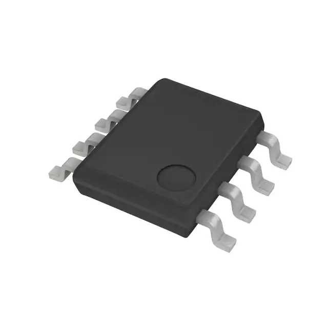
STMicroelectronics TSB712AIST

Part No.:
TSB712AIST
Manufacturer:
STMicroelectronics
Category:
Instrumentation, Op Amps, Buffer Amps
Package:
8-TSSOP, 8-MSOP (0.118", 3.00mm Width)
Datasheet:
AetrixTSB712AIST.pdf
Description:
IC OPAMP GP 2 CIRCUIT 8MINISO
Quantity:
Payment:
Payment
Shipping:
Shipping

Inventory:3,980

Please send an inquiry. Send us your inquiry, and we will respond immediately.

Part Number
Quantity*
Price
Name*
Company
Email*
Comments

Product details

Overview

TSB712AIST from STMicroelectronics is a dual-channel, rail-to-rail input/output precision operational amplifier optimized for high-accuracy current sensing and industrial signal conditioning. It delivers 6 MHz gain bandwidth, 3 V/µs slew rate, 300 µV max input offset voltage at 25 °C, and operates from 2.7 V to 36 V single supply (±1.35 V to ±18 V dual). It is used in automotive-grade motor control feedback loops where wide common-mode range and EMI robustness are critical.

For engineers reviewing the TSB712AIST datasheet, TSB712AIST pinout, TSB712AIST application, or TSB712AIST equivalent, key selection criteria include its guaranteed rail-to-rail input stage up to VCC+ +0.1 V, integrated EMI filter, 2 kV HBM ESD rating, -40 °C to +125 °C extended temperature operation, and dual-channel SO8 packaging for space-constrained PCB layouts.

Technical Context

The TSB712AIST employs a complementary NPN/PNP rail-to-rail input stage enabling full common-mode range from VCC− to VCC+ +0.1 V, with optimal performance maintained from VCC− to VCC+ −1.5 V. Its architecture avoids phase reversal across the absolute maximum input range and supports stable operation into 100 pF capacitive loads.

It features an integrated EMI filter that suppresses RF rectification-induced offset shifts, validated by EMIRR characterization. The device maintains 115 dB CMRR and 125 dB PSRR over temperature, with low 12 nV/√Hz input voltage noise at 10 kHz and 0.57 µV/√month long-term offset drift stability.

Key Specifications

ParameterValue and Actual Design Meaning
Gain Bandwidth Product6 MHz - enables stable closed-loop operation up to 100 kHz with gain ≥60, suitable for fast current loop compensation.
Input Offset Voltage±300 µV max at 25 °C - ensures ≤0.3 mV error in 10 V full-scale measurement, critical for <0.01% accuracy systems.
Slew Rate3 V/µs - supports 10 V step response in <3.4 µs, sufficient for 100 kHz PWM-based motor control feedback.
Supply Voltage Range2.7 V to 36 V - allows direct interface with 12 V/24 V industrial buses and battery-powered sensors without LDO pre-regulation.
Input Voltage Noise12 nV/√Hz at 10 kHz - minimizes contribution to total system noise floor in strain gauge and Hall sensor front-ends.
EMI RejectionIntegrated on-chip EMI filter - eliminates need for external RC filters, reducing board area and preserving phase margin in noisy environments.
ESD Tolerance2 kV HBM - meets IEC 61000-4-2 Level 3 requirements for industrial equipment without additional protection circuitry.
Operating Temperature-40 °C to +125 °C - qualified for under-hood automotive and factory-floor industrial deployments without derating.

Pinout & Package

TSB712AIST is housed in a MiniSO-8 (SO8) surface-mount package with exposed pad for thermal enhancement and standard JEDEC MS-012AC footprint compatibility.

Pin/TerminalCircuit RoleDesign Meaning
1 OUT1Output channel 1Capable of sourcing/sinking 20 mA at full rail, supporting direct drive of ADC reference buffers or low-side shunt amplifiers.
2 IN1−Inverting input channel 1Protected by internal ESD diodes to rails; differential input voltage limited to ±2 V to prevent damage during saturation events.
3 IN1+Non-inverting input channel 1Part of rail-to-rail input pair; bias current polarity flips near VCC+ due to PNP/NPN transition-avoid operation within 1 V of positive rail.
4 VCC−Negative supply voltageReference node for dual-supply operation; must be connected even in single-supply use to ensure proper internal biasing.
5 IN2+Non-inverting input channel 2Independent channel enabling dual-path signal conditioning-e.g., simultaneous high-side and low-side current sensing in three-phase inverters.
6 IN2−Inverting input channel 2Matched to IN1− for channel-to-channel crosstalk <100 dB at 10 kHz, ensuring isolation in multi-sensor data acquisition.
7 OUT2Output channel 2Electrically isolated output stage; supports independent load driving without interaction-critical for redundant safety monitoring paths.
8 VCC+Positive supply voltageAccepts up to +40 V transient-enables robust operation in 24 V systems subject to load-dump transients per ISO 7637-2.

Key Features

FeatureDesign Value
Rail-to-rail input stageCommon-mode range extends to VCC+ +0.1 V, eliminating level-shifting circuits in high-side current sensing topologies.
Low input offset drift2.8 µV/°C max over −40 °C to +125 °C - reduces thermal error to <0.23 mV across full temperature span in 85 °C ambient rise.
High PSRR & CMRR125 dB PSRR and 130 dB CMRR at DC - rejects supply ripple and common-mode interference in noisy PLC analog input modules.
Stable capacitive load drive100 pF minimum stable load - permits direct connection to long traces or ADC input capacitance without external isolation resistors.
Automotive qualificationAEC-Q100 Grade 1 compliant - certified for engine control units, battery management systems, and ADAS power stages.
Low THD+N0.0003% at 1 kHz - preserves signal fidelity in precision instrumentation and audio-grade test equipment front-ends.

Applications

High-Side Current SensingHall Effect Sensor Signal Conditioning

Use Scenario: Monitoring phase current in 24 V BLDC motor drives using shunt resistor placed between power supply and high-side FET source.

IC Role / Device Role / Timing Role: Dual op-amp configured as difference amplifier (CH1) and reference buffer (CH2), rejecting common-mode bus voltage up to 24 V while amplifying mV-level shunt drops.

Use Value: Enables accurate torque control with <0.5% gain error over temperature, leveraging rail-to-rail inputs to capture full dynamic range without clipping.

Use Scenario: Amplifying low-amplitude analog output from linear Hall effect sensors in automotive throttle position and pedal angle detection.

IC Role / Device Role / Timing Role: Single-ended amplifier with gain of 100, rejecting EMI from adjacent ignition coils and alternator noise via integrated filter and 125 dB PSRR.

Use Value: Delivers sub-degree angular resolution by maintaining 12 nV/√Hz noise floor and <300 µV offset-critical for ASIL-B functional safety compliance.

Data Acquisition Front-EndIndustrial Process Control Loop

Use Scenario: Simultaneous acquisition of four 4–20 mA loop signals in modular PLC I/O cards with 16-bit SAR ADCs.

IC Role / Device Role / Timing Role: Two TSB712AIST devices per card provide eight channels of rail-to-rail buffering, each driving 10 kΩ ADC input with <1 LSB error.

Use Value: Achieves 16-bit effective resolution by limiting total input-referred error to <15 µV RMS across −40 °C to +70 °C operating range.

Use Scenario: Closed-loop pressure regulation in chemical dosing pumps using strain gauge bridge and PID controller on microcontroller.

IC Role / Device Role / Timing Role: Instrumentation amplifier front-end (gain = 1000) with matched dual channels for bridge excitation and differential output amplification.

Use Value: Maintains 0.05% linearity over 10:1 turndown ratio by suppressing thermal EMF errors via low 2.8 µV/°C drift and 130 dB CMRR.

Equivalent & Alternatives

The following parts are listed as comparable options for similar dual-channel precision op amp applications.

Alternative PartTechnical DifferenceApplication DifferenceSelection Advice
TSB712ISTHigher max input offset voltage (±800 µV vs. ±300 µV at 25 °C); same package and pinout.Less suitable for <0.01% accuracy current sensing but acceptable for general-purpose industrial amplification.Select TSB712IST only when cost sensitivity outweighs precision requirements and system calibration compensates for higher initial offset.
TSB512IDTSame 36 V rating and rail-to-rail I/O, but lower GBP (2.5 MHz) and higher input noise (25 nV/√Hz).Better suited for low-power, battery-operated sensors where 1.4 mA supply current matters more than bandwidth.Choose TSB512IDT for portable test equipment needing extended battery life, not for high-speed motor control feedback paths.

Compared with TSB712IST, the TSB712AIST provides tighter initial offset and lower drift-critical for uncalibrated systems-while TSB512IDT trades bandwidth and noise performance for 40% lower quiescent current, making it viable only in low-frequency, power-constrained designs.

Availability

TSB712AIST is available at Aetrix Electronics and suitable for high-side current sensing, Hall effect sensor interfaces, industrial data acquisition, and motor control applications requiring stable component supply across automotive and industrial lifecycles.

Supply support for TSB712AIST includes scheduled delivery planning, volume procurement assistance, BOM continuity management, traceable sourcing, and lifecycle availability coordination for OEM customers, industrial embedded developers, connected-device designers, and electronics production programs.

Manufacturer

STMicroelectronics is a global semiconductor leader headquartered in Geneva, Switzerland, designing and manufacturing microcontrollers, power management ICs, analog chips, and MEMS sensors for industrial, automotive, and consumer markets.

The TSB712AIST belongs to ST's high-voltage precision op amp product line, engineered specifically for demanding industrial and automotive signal conditioning where rail-to-rail operation, EMI resilience, and extended temperature reliability are mandatory.

FAQ

What is the maximum capacitive load the TSB712AIST can drive stably?

The TSB712AIST is characterized for stable operation with up to 100 pF capacitive load at unity gain, as confirmed in Figure 26 of DS12487. Driving larger loads requires external series resistance (≥10 Ω) at the output to maintain ≥45° phase margin, especially at 36 V supply where parasitic inductance increases risk of oscillation.

Does the TSB712AIST support true rail-to-rail output swing under 15 mA load?

Yes-TSB712AIST guarantees high-level output voltage drop ≤200 mV and low-level output voltage rise ≤200 mV at ISINK/ISOURCE = 15 mA and −40 °C to +125 °C, per Table 5. This enables full 0–24 V output swing in 24 V single-supply systems when driving typical ADC reference buffers or comparator inputs.

How does the integrated EMI filter function without external components?

The EMI filter is implemented as on-die RC networks tied to internal bias nodes, attenuating RF energy above 100 MHz before it reaches the input differential pair. This prevents rectification-induced offset shifts observed in non-filtered op amps, eliminating need for external 100 Ω + 1 nF R-C filters typically required for CISPR-25 Class 5 compliance in automotive ECUs.

Can the TSB712AIST be used in single-supply comparator mode?

No-though it has rail-to-rail inputs, the TSB712AIST is not designed for open-loop comparator operation. Its internal compensation and lack of built-in hysteresis make it susceptible to oscillation and slow recovery from saturation. For comparator functions, ST recommends dedicated devices like TS882 or TLV3201 with defined propagation delay and internal hysteresis.

TSB712AIST Specifications

Product attributes
Attribute value
Manufacturer:
STMicroelectronics
Series:
-
Package/Case:
8-TSSOP, 8-MSOP (0.118", 3.00mm Width)
Packaging:
Tape & Reel (TR)
Product Status:
Active
Amplifier Type:
General Purpose
Number of Circuits:
2
Output Type:
Rail-to-Rail
Slew Rate:
3V/µs
Gain Bandwidth Product:
6 MHz
-3db Bandwidth:
-
Current - Input Bias:
300 nA
Voltage - Input Offset:
650 µV
Current - Supply:
1.8mA
Current - Output / Channel:
50 mA
Voltage - Supply Span (Min):
2.7 V
Voltage - Supply Span (Max):
36 V
Operating Temperature:
-40°C ~ 125°C
Grade:
Automotive
Qualification:
AEC-Q100
Mounting Type:
Surface Mount
Supplier Device Package:
8-MiniSO

TSB712AIST FAQ

1.How can I place an order for TSB712AIST through Aetrix?

Please submit a Request for Quotation (RFQ) for TSB712AIST on Aetrix. Our sales agent will provide a competitive quotation and guide you through the order confirmation once you accept the terms.

2.Are the price and stock information for TSB712AIST reliable?

The price and inventory of TSB712AIST are updated periodically and may fluctuate due to market conditions. Stock and pricing data are typically refreshed every 24 hours. Quotation validity for TSB712AIST is usually 5 days.

3.What payment methods are accepted for TSB712AIST?

We accept Wire Transfer, PayPal, Credit Card, Western Union, MoneyGram, and Escrow for TSB712AIST transactions.

Note: Certain payment methods may incur a processing fee.

4.How is shipping managed for TSB712AIST?

TSB712AIST orders can be shipped via leading logistics carriers, including DHL, UPS, FedEx, TNT, or Registered Mail.

Once your TSB712AIST order is processed, you will receive an email with the shipment details and tracking number.

Note: Tracking information may take up to 24 hours to appear. Express delivery typically takes 3–5 business days.

5.How can I obtain technical support or documentation for TSB712AIST?

For technical support, including TSB712AIST datasheets, pinout diagrams, or application guidance, please contact our engineering support team. They can provide detailed documentation and assistance for your TSB712AIST requirements.

6.How does Aetrix verify that TSB712AIST is sourced from the original manufacturer or authorized distributors?

All TSB712AIST products on Aetrix are procured from qualified distributors and authorized channels. Our dedicated quality assurance team conducts strict verification, including traceability checks and, if necessary, third-party testing. This ensures that TSB712AIST meets industry standards.

7.What is the process for return or replacement of TSB712AIST?

All TSB712AIST units undergo pre-shipment inspection (PSI). If there is an issue with TSB712AIST, returns or replacements are accepted under the following conditions:

1.Quantity discrepancies, incorrect items, or visible external defects (such as breakage or corrosion), acknowledged by Aetrix.

2.The issue is reported within 90 days of delivery.

3.The TSB712AIST part is unused and in its original packaging.

Return procedure for TSB712AIST:

1.Submit a request within 90 days.

2.Obtain a Return Material Authorization (RMA) from Aetrix.

TSB712AIST Tags

  • TSB712AIST
  • TSB712AIST PDF
  • TSB712AIST Datasheet
  • TSB712AIST Specifications
  • TSB712AIST Images
  • STMicroelectronics
  • STMicroelectronics TSB712AIST
  • Buy TSB712AIST
  • TSB712AIST Price
  • TSB712AIST Distributor
  • TSB712AIST Supplier
  • TSB712AIST Wholesale
Related Products
LM358DT
LM358DT

STMicroelectronics

LM358DR
LM358DR

Texas Instruments

LM2904DR
LM2904DR

Texas Instruments

LM358ADR
LM358ADR

Texas Instruments

LM2904DGKR
LM2904DGKR

Texas Instruments

LM324DR
LM324DR

Texas Instruments

MCP6006T-E/OT
MCP6006T-E/OT

Microchip Technology

MCP6006UT-E/OT
MCP6006UT-E/OT

Microchip Technology

LM324PWR
LM324PWR

Texas Instruments

LM2902PWR
LM2902PWR

Texas Instruments

LM2902DR
LM2902DR

Texas Instruments

LM358P
LM358P

Texas Instruments

Tech Hub

Search

Search

PRODUCT

PRODUCT

PHONE

PHONE

USER

USER