Silicon Labs TSM6025BEUR+T
- Part No.:
- TSM6025BEUR+T
- Manufacturer:
- Silicon Labs
- Category:
- Voltage Reference
- Package:
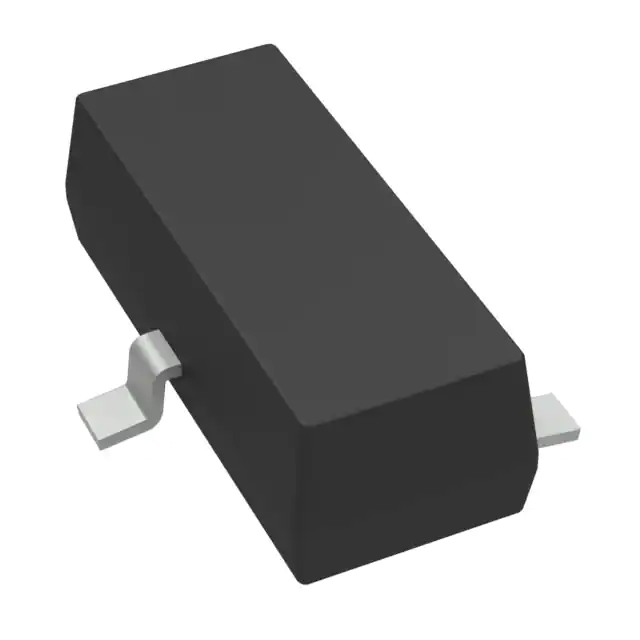
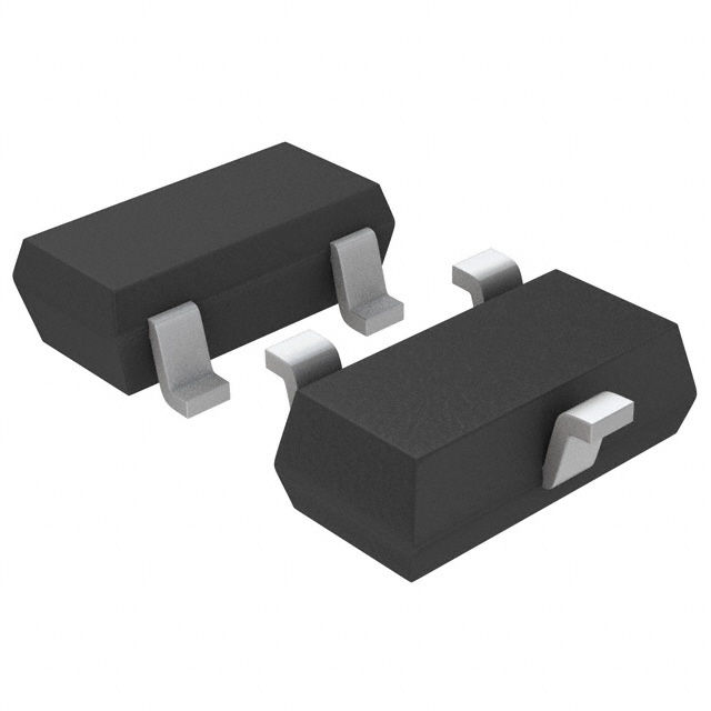
- TO-236-3, SC-59, SOT-23-3
- Datasheet:
-
TSM6025BEUR+T.pdf
- Description:
- IC VREF SERIES 0.4% SOT23-3
- Quantity:
- Payment:

- Shipping:

Inventory:3,244
Please send an inquiry. Send us your inquiry, and we will respond immediately.
Product details
Overview
TSM6025BEUR+T from Silicon Laboratories is a 3-terminal, series-mode 2.5 V precision voltage reference with 0.4% initial accuracy, 25 ppm/°C max temperature coefficient, and ±500 μA output drive capability. It operates from 2.7 V to 12.6 V input, delivers low dropout (100 mV at 500 μA), and targets high-accuracy analog signal chains in battery-powered instrumentation and industrial transmitters.
For engineers reviewing the TSM6025BEUR+T datasheet, TSM6025BEUR+T pinout, TSM6025BEUR+T application, or TSM6025BEUR+T equivalent, key selection criteria include initial accuracy vs. temperature drift trade-offs, capacitive-load stability up to 2200 pF, quiescent current ≤35 μA, and compatibility with low-headroom 3V/5V systems requiring stable 2.5 V references.
Technical Context
The TSM6025BEUR+T integrates a proprietary low-drift bandgap core followed by a unity-gain output amplifier optimized for low headroom and wide capacitive-load tolerance. Its series-mode architecture eliminates external bias resistors and ensures supply current remains stable across input voltage variations (ΔIIN/ΔVIN < 2.0 μA/V).
It achieves thermal stability via matched transistor design and stress-compensated packaging, delivering 130 ppm typical temperature hysteresis and 50 ppm/1000 hr long-term drift. The output stage supports bidirectional 500 μA load current without external compensation while maintaining 0.14 μV/μA load regulation and 140 μV/V line regulation.
Key Specifications
| Parameter | Value and Actual Design Meaning |
|---|---|
| Output Voltage | 2.500 V ±0.4% at +25°C - guarantees absolute accuracy within ±10 mV for calibration-critical ADC/DAC biasing |
| Temp Coefficient | 25 ppm/°C max (–40°C to +85°C) - limits output drift to ±2.1 mV over full industrial temperature range |
| Quiescent Current | 35 μA max - enables multi-year operation from coin-cell batteries in portable data loggers |
| Dropout Voltage | 100 mV at 500 μA load - allows use with 2.6 V supplies in ultra-low-voltage 3V systems |
| Capacitive Load Stability | 0–2200 pF - eliminates need for external compensation, simplifying layout in noise-sensitive sensor front-ends |
| Line Regulation | 140 μV/V - ensures <0.35 mV output shift per volt of input variation, critical for unregulated power rails |
| Load Regulation | 0.14 μV/μA sourcing - maintains sub-70 μV error across full 500 μA load range, supporting precision current sources |
Pinout & Package
Supplied in a 3-pin SOT23 package (2.92 mm × 1.3 mm × 1.0 mm), the TSM6025BEUR+T uses standard JEDEC MO-203AA outline with gull-wing leads and RoHS-compliant lead-free finish.
| Pin/Terminal | Circuit Role | Design Meaning |
|---|---|---|
| 1 (IN) | Supply Input | Accepts 2.7 V to 12.6 V; internal series regulator draws only 35 μA regardless of VIN - no external resistor required |
| 2 (OUT) | 2.5 V Reference Output | Provides low-impedance, bidirectional ±500 μA drive; stable with 0–2200 pF capacitive loads |
| 3 (GND) | Analog Ground Reference | Must be connected to clean system ground plane; separates reference return from digital or power ground currents |
Key Features
| Feature | Design Value |
|---|---|
| Precision Bandgap Core | Proprietary topology achieving 25 ppm/°C max drift and 0.4% initial accuracy without laser trimming |
| Series-Mode Architecture | Eliminates external bias resistor and associated tolerance/temperature errors - improves system-level accuracy |
| Low Dropout Operation | 100 mV dropout at 500 μA enables direct use after LDOs or from marginal 3V rails |
| Wide Capacitive-Load Tolerance | Stable with 0–2200 pF output capacitance - removes need for isolation resistors in filter-heavy ADC inputs |
| Ultra-Low Supply Current Drift | ΔIIN/ΔVIN < 2.0 μA/V - ensures consistent power budget across varying input conditions |
Applications
| Industrial Process Transmitters | Battery-Powered Data Acquisition |
|---|---|
Use Scenario: 4–20 mA loop-powered smart sensors measuring pressure, temperature, or flow in hazardous environments. IC Role / Device Role / Timing Role: Primary 2.5 V reference for 16-bit DAC and sigma-delta ADC, enabling <±0.1% total measurement uncertainty. Use Value: 25 ppm/°C tempco and 0.4% initial accuracy ensure field calibration holds over –40°C to +85°C ambient without recalibration. | Use Scenario: Portable handheld multimeter or environmental logger powered by CR2032 coin cell. IC Role / Device Role / Timing Role: Precision voltage reference for auto-ranging ADC and internal self-calibration circuitry. Use Value: 35 μA quiescent current extends battery life beyond 5 years; 2200 pF load stability allows direct connection to ADC input capacitor without buffer. |
| Hard-Disk Drive Servo Control | Precision 3V/5V Systems |
Use Scenario: Position error signal (PES) generation in HDD voice-coil motor control loops. IC Role / Device Role / Timing Role: Stable 2.5 V reference for differential amplifiers and comparator thresholds in servo channel ICs. Use Value: 140 μV/V line regulation prevents PES offset shifts during rapid spindle voltage transients; 0.14 μV/μA load regulation maintains accuracy under dynamic current demands. | Use Scenario: High-resolution medical sensor interface (e.g., ECG front-end) operating from regulated 3.3 V rail. IC Role / Device Role / Timing Role: Low-noise 2.5 V reference for instrumentation amplifier gain-setting and ADC reference input. Use Value: 50 μVP-P (0.1–10 Hz) and 125 μVRMS (10 Hz–10 kHz) noise support 20+ ENOB; 100 mV dropout allows operation even if 3.3 V rail sags to 2.6 V. |
Equivalent & Alternatives
The following parts are listed as comparable options for similar precision voltage reference applications.
| Alternative Part | Technical Difference | Application Difference | Selection Advice |
|---|---|---|---|
| MAX6025BEUR+T | Pin-for-pin compatible; identical 0.4% accuracy and 25 ppm/°C spec; same SOT23-3 package and electrical behavior | No functional or layout changes required; drop-in replacement verified by Silicon Labs documentation | Select when legacy MAXIM design reuse or dual-sourcing strategy is required |
| REF3025AIDBZR | 0.2% initial accuracy, 50 ppm/°C max tempco; 45 μA max IQ; requires ≥1.5 V headroom (dropout ~150 mV at 500 μA) | Higher accuracy but worse tempco; slightly higher quiescent current; less tolerant of low-input-voltage conditions | Select when tighter initial tolerance is prioritized over temperature stability and ultra-low dropout |
Compared with MAX6025BEUR+T, the TSM6025BEUR+T offers identical performance and footprint, enabling seamless second-source qualification; versus REF3025AIDBZR, it trades 0.2% initial accuracy for superior thermal stability and lower dropout-critical in wide-temperature industrial deployments.
Availability
TSM6025BEUR+T is available at Aetrix Electronics and suitable for industrial process transmitters, battery-powered data acquisition systems, and precision 3V/5V analog signal chains requiring stable component supply across extended product lifecycles.
Supply support for TSM6025BEUR+T includes scheduled delivery planning, volume procurement assistance, BOM continuity management, traceable sourcing, and lifecycle availability coordination for OEM customers, industrial embedded developers, connected-device designers, and electronics production programs.
Manufacturer
Silicon Laboratories is a U.S.-based semiconductor company specializing in precision analog, timing, and mixed-signal ICs for industrial, communications, and consumer applications.
The TSM6025BEUR+T belongs to Silicon Labs' precision voltage reference product line, engineered specifically for high-accuracy, low-power, and thermally robust operation in harsh industrial and portable measurement systems.
FAQ
What is the guaranteed initial accuracy of the TSM6025BEUR+T over temperature?
The TSM6025BEUR+T guarantees ±0.4% initial output voltage accuracy at +25°C, with full specification over –40°C to +85°C. Its maximum temperature coefficient is 25 ppm/°C across that range, resulting in a worst-case total drift of ±2.1 mV. This performance is validated per the "box method" defined in the datasheet and applies directly to the TSM6025BEUR+T device marking ACY.
Can the TSM6025BEUR+T drive a 1000 pF capacitive load without oscillation?
Yes, the TSM6025BEUR+T is fully stable with capacitive loads from 0 pF up to 2200 pF, including 1000 pF. No external series resistor or compensation network is required. This capability is confirmed in the Electrical Characteristics table (Capacitive-Load Stability Range = 0–2.2 nF) and supported by the internal frequency compensation design described in the Theory of Operation section of the TSM6025BEUR+T datasheet.
How does the supply current of the TSM6025BEUR+T vary with input voltage?
The TSM6025BEUR+T exhibits minimal supply current variation with input voltage: ΔIIN/ΔVIN is guaranteed ≤2.0 μA/V across its full operating range (VOUT + 0.2 V ≤ VIN ≤ 12.6 V). At nominal conditions (VIN = 5 V), quiescent current is typically 27 μA and never exceeds 35 μA - a key advantage of its series-mode architecture over shunt references.
Is the TSM6025BEUR+T pin-compatible with the MAX6025 series?
Yes, the TSM6025BEUR+T is explicitly designed as a pin-for-pin alternate source for the MAX6025 voltage reference. Both devices use identical 3-pin SOT23 packaging, share identical pin functions (IN, OUT, GND), and match on all key electrical parameters including accuracy, tempco, dropout, and load drive. Silicon Labs confirms this compatibility in the TSM6025BEUR+T product description and features list.
What is the maximum continuous output current the TSM6025BEUR+T can source or sink?
The TSM6025BEUR+T can continuously source or sink up to ±500 μA while maintaining specified accuracy and stability. This is confirmed in both the Features list ("Output Source/Sink Current: ±500μA") and the Electrical Characteristics table (Load Regulation test conditions). Exceeding this current may degrade output voltage regulation or increase dropout beyond specifications.
TSM6025BEUR+T Specifications
- Product attributes
- Attribute value
- Manufacturer:
- Silicon Labs
- Package/Case:
- TO-236-3, SC-59, SOT-23-3
- Series:
- -
- Packaging:
- Tape & Reel (TR)
- Product Status:
- Obsolete
- Reference Type:
- Series
- Output Type:
- Fixed
- Voltage - Output (Min/Fixed):
- 2.5V
- Voltage - Output (Max):
- -
- Current - Output:
- 500 µA
- Tolerance:
- ±0.4%
- Temperature Coefficient:
- 30ppm/°C
- Noise - 0.1Hz to 10Hz:
- 50µVp-p
- Noise - 10Hz to 10kHz:
- 125µVrms
- Voltage - Input:
- 2.7V ~ 12.6V
- Current - Supply:
- 35µA
- Current - Cathode:
- -
- Operating Temperature:
- -40°C ~ 85°C (TA)
- Grade:
- -
- Qualification:
- -
- Mounting Type:
- Surface Mount
- Supplier Device Package:
- SOT-23-3
TSM6025BEUR+T FAQ
1.How can I place an order for TSM6025BEUR+T through Aetrix?
Please submit a Request for Quotation (RFQ) for TSM6025BEUR+T on Aetrix. Our sales agent will provide a competitive quotation and guide you through the order confirmation once you accept the terms.
2.Are the price and stock information for TSM6025BEUR+T reliable?
The price and inventory of TSM6025BEUR+T are updated periodically and may fluctuate due to market conditions. Stock and pricing data are typically refreshed every 24 hours. Quotation validity for TSM6025BEUR+T is usually 5 days.
3.What payment methods are accepted for TSM6025BEUR+T?
We accept Wire Transfer, PayPal, Credit Card, Western Union, MoneyGram, and Escrow for TSM6025BEUR+T transactions.
Note: Certain payment methods may incur a processing fee.
4.How is shipping managed for TSM6025BEUR+T?
TSM6025BEUR+T orders can be shipped via leading logistics carriers, including DHL, UPS, FedEx, TNT, or Registered Mail.
Once your TSM6025BEUR+T order is processed, you will receive an email with the shipment details and tracking number.
Note: Tracking information may take up to 24 hours to appear. Express delivery typically takes 3–5 business days.
5.How can I obtain technical support or documentation for TSM6025BEUR+T?
For technical support, including TSM6025BEUR+T datasheets, pinout diagrams, or application guidance, please contact our engineering support team. They can provide detailed documentation and assistance for your TSM6025BEUR+T requirements.
6.How does Aetrix verify that TSM6025BEUR+T is sourced from the original manufacturer or authorized distributors?
All TSM6025BEUR+T products on Aetrix are procured from qualified distributors and authorized channels. Our dedicated quality assurance team conducts strict verification, including traceability checks and, if necessary, third-party testing. This ensures that TSM6025BEUR+T meets industry standards.
7.What is the process for return or replacement of TSM6025BEUR+T?
All TSM6025BEUR+T units undergo pre-shipment inspection (PSI). If there is an issue with TSM6025BEUR+T, returns or replacements are accepted under the following conditions:
1.Quantity discrepancies, incorrect items, or visible external defects (such as breakage or corrosion), acknowledged by Aetrix.
2.The issue is reported within 90 days of delivery.
3.The TSM6025BEUR+T part is unused and in its original packaging.
Return procedure for TSM6025BEUR+T:
1.Submit a request within 90 days.
2.Obtain a Return Material Authorization (RMA) from Aetrix.
TSM6025BEUR+T Tags
-
TL431AIDBZR
Texas Instruments
-
TL431BQDBZR
Texas Instruments

-
AN431AN-ATRG1
Diodes Incorporated

-
LM4040CYM3-2.5-TR
Microchip Technology
-
LM4040CYM3-4.1-TR
Microchip Technology
-
LM4040EIM3-2.5/NOPB
Texas Instruments

-
AZ431LBNTR-G1
Diodes Incorporated
-
LM4040D20IDBZR
Texas Instruments
-
LM4041DIM3-ADJ/NOPB
Texas Instruments
-
LM4040DIM3X-2.5/NOPB
Texas Instruments
-
LM4040DIM3-2.5/NOPB
Texas Instruments

-
AZ431LANTR-G1
Diodes Incorporated
Tech Hub

Comparator circuit design covering voltage thresholds, input limits, open-collector outputs, LM393 wiring, op-amp differences, hysteresis, timing, window detection and practical fault diagnosis.
Schmitt triggers use separate rising and falling thresholds to stabilize slow or noisy signals. This guide covers hysteresis, 74HC14 and 74HCT14 selection, comparator calculations, RC oscillators and p…
Counterfeit components can hide behind convincing markings and passing basic function tests. This engineering reference covers source traceability, external inspection, X-ray, XRF, electrical testing, …
A practical engineering and sourcing framework covering lifecycle verification, lifetime-buy calculations, replacement qualification, supplier checks and counterfeit-risk controls.
TTL and CMOS logic families differ in thresholds, loading, output drive, power and timing. This engineering guide compares 74HC and 74HCT, calculates noise margins and checks 3.3 V/5 V compatibility.
A practical engineering guide to 3.3V and 5V logic compatibility, input thresholds, resistor dividers, translator ICs, MOSFET level shifting, I2C pull-ups, timing limits and power-sequencing risks.
The 74HC595 uses push-pull logic outputs, while the TPIC6B595 uses 50 V open-drain DMOS sinks for higher-power loads. This guide compares timing, current limits, 3.3 V interfacing, load wiring, thermal…
The 74HC595 converts serial data into eight stable parallel outputs. This guide covers pin functions, shift and storage timing, OE and MR behavior, drive-current limits, cascading, voltage compatibilit…
A technical comparison of level-sensitive latches and edge-triggered flip-flops, covering timing windows, setup and hold limits, master–slave operation, time borrowing, race-through, HDL inference and…
A D latch stores one bit while Enable controls when data can pass. This reference covers gate-level operation, truth tables, transparency, setup and hold timing, LE versus OE, common ICs and practical …









