Send an Inquiry

To receive a quote for your project, please fill in the following information, and we’ll get back to you promptly.

Name*
Company*
Email Address*
Phone/WhatsApp
Part Number*
Quantity*
Message
Submit Inventory List

Please fill in the following information, and we’ll get back to you promptly.

Name*
Company*
Email Address*
Phone/WhatsApp
Upload My List
Message

Silicon Labs TSM984ESE+

Part No.:
TSM984ESE+
Manufacturer:
Silicon Labs
Category:
Comparators
Package:
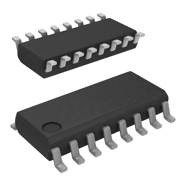
16-SOIC (0.154", 3.90mm Width)
Datasheet:
AetrixTSM984ESE+.pdf
Description:
IC COMPARATR 4 W/VOLT REF 16SOIC
Quantity:
Payment:
Payment
Shipping:
Shipping

Inventory:1,627

Please send an inquiry. Send us your inquiry, and we will respond immediately.

Part Number
Quantity*
Price
Name*
Company
Email*
Comments

Product details

Overview

TSM984ESE+ from Silicon Laboratories is a quad micropower analog comparator with integrated 1.182V ±2% reference, open-drain outputs, and ultra-low quiescent current of 8.5μA (max) over –40°C to +85°C. It operates from single +2.5V to +11V or dual ±1.25V to ±5.5V supplies, features input voltage range extending to V– and within 1.3V of V+, and supports wired-OR logic in battery-powered threshold detection systems.

For engineers reviewing the TSM984ESE+ datasheet, TSM984ESE+ pinout, TSM984ESE+ application, or TSM984ESE+ equivalent, key selection criteria include its quad-channel open-drain architecture, internal reference accuracy and temperature drift, supply current vs. temperature behavior, and GND-referenced output capability enabling direct TTL/CMOS interfacing without level-shifting components.

Technical Context

The TSM984ESE+ integrates four independent comparators sharing a single 1.182V reference referenced to V–, with each output sinking to GND (not V–), enabled by dedicated GND and V– pins. Its input common-mode range spans from V– to (V+ – 1.3V), supporting rail-to-rail sensing in low-voltage systems down to 2.5V (with functional operation down to 1.5V for comparators only).

Unlike TSM972/TSM973/TSM982 variants, the TSM984ESE+ lacks an adjustable HYST pin and does not support internal hysteresis programming; hysteresis must be implemented externally via positive feedback. Propagation delay is 12μs (high-to-low) at 10mV overdrive with 1MΩ pullup and 100pF load.

Key Specifications

Parameter Value and Actual Design Meaning
Supply Voltage Range +2.5V to +11V (single) or ±1.25V to ±5.5V (dual); enables compatibility with 3V/5V logic rails and legacy ±5V systems.
Quiescent Current 8.5μA max over –40°C to +85°C; ensures multi-year battery life in always-on sensor monitoring nodes.
Reference Voltage 1.182V ±2% over –40°C to +85°C; provides stable trip-point generation without external precision references.
Input Common-Mode Range V– to (V+ – 1.3V); allows direct sensing of signals near ground or supply rails without attenuation networks.
Propagation Delay 12μs high-to-low at 10mV overdrive; supports response-critical window detection in power sequencing and fault monitoring.
Output Type Open-drain, sink-to-GND; enables wired-OR combining of multiple comparators and level translation to any logic family.
Package 16-pin SOIC; industry-standard footprint compatible with automated assembly and thermal management up to 696mW at +70°C.

Pinout & Package

Package: 16-pin SOIC (width 7.5mm, JEDEC MS-013 compliant), rated for –40°C to +85°C operating temperature.

Pin Circuit Role Design Meaning
1 OUTB Comparator B open-drain output; sinks to GND-enables direct connection to microcontroller interrupt inputs or LED drivers.
2 OUTA Comparator A open-drain output; independently controllable for dual-threshold detection (e.g., under/overvoltage).
3 V+ Positive supply input; accepts up to +11V or +5.5V in dual-supply mode-supports wide-input industrial power rails.
4 INA− Inverting input for Comparator A; high-impedance (±0.01nA leakage) for minimal loading of sensor dividers.
5 INA+ Noninverting input for Comparator A; matched offset (±10mV) with INA− for precise differential thresholding.
6 INB− Inverting input for Comparator B; electrically identical to INA−-allows parallel configuration for redundancy or averaging.
7 INB+ Noninverting input for Comparator B; supports independent signal routing for multi-zone monitoring (e.g., temp/voltage).
8 REF 1.182V reference output referenced to V−; sources/sinks up to 25μA/15μA-drives external resistor networks for hysteresis.
9 V− Negative supply input; tied to GND in single-supply mode; enables true dual-supply operation down to ±1.25V.
10 INC− Inverting input for Comparator C; identical electrical specs to INA−-extends monitoring to third independent channel.
11 INC+ Noninverting input for Comparator C; supports cascaded or sequential decision logic across all four comparators.
12 IND− Inverting input for Comparator D; enables full quad-threshold detection (e.g., 4-level battery SOC indication).
13 IND+ Noninverting input for Comparator D; completes independent input pair set-no shared inputs between comparators.
14 GND Ground reference pin; separate from V−-ensures clean output switching and eliminates ground bounce in mixed-signal layouts.
15 OUTD Comparator D open-drain output; sinks to GND-supports OR-ing with OUTA/OUTB/OUTC for system-level fault aggregation.
16 OUTC Comparator C open-drain output; fully isolated from other outputs-allows independent control of discrete loads or indicators.

Key Features

Feature Design Value
Quad comparator + reference in one package Reduces BOM count and PCB area vs. discrete solutions-ideal for space-constrained portable instrumentation.
Ultra-low 8.5μA max supply current Extends battery runtime in wireless sensors and wearables where duty cycling cannot eliminate baseline consumption.
GND-referenced open-drain outputs Eliminates need for external level shifters when interfacing with 3.3V/5V microcontrollers-simplifies IO design.
1.182V ±2% internal reference Removes external voltage reference IC and associated decoupling-lowers cost and improves long-term stability.
Input range includes negative supply rail Enables direct sensing of bipolar signals (e.g., op-amp outputs, transducer bridges) without AC coupling or biasing.
16-pin SOIC with 696mW power dissipation Supports higher ambient temperatures in industrial enclosures without derating concerns or heatsinking.

Applications

Overvoltage/Undervoltage Protection Battery Fuel Gauging

Use Scenario: Monitoring DC input rails in embedded power supplies to trigger shutdown before damage occurs.

IC Role / Device Role / Timing Role: Quad comparator implements independent high/low thresholds per rail, with REF providing stable trip points.

Use Value: Eliminates need for external reference and reduces component count by 4× vs. single-comparator solutions.

Use Scenario: Segmenting lithium-ion battery voltage into 4 discrete state-of-charge (SOC) bands for LED status indication.

IC Role / Device Role / Timing Role: Each comparator monitors a unique voltage band using resistor-divider scaling against REF.

Use Value: Achieves <1% threshold error across –40°C to +85°C without calibration-reducing firmware complexity.

Industrial Sensor Threshold Detection Level Translation Interface

Use Scenario: Converting analog sensor outputs (e.g., pressure, temperature) into digital alerts for PLC inputs.

IC Role / Device Role / Timing Role: Four comparators process parallel sensor channels, with open-drain outputs wired-OR'd to a single interrupt line.

Use Value: Reduces wiring and I/O pin count on host controller while maintaining deterministic response time (<12μs).

Use Scenario: Translating ±5V industrial bus signals (e.g., RS-422, analog sensor outputs) to 3.3V logic levels for MCU ADC inputs.

IC Role / Device Role / Timing Role: TSM984ESE+ acts as a rail-to-rail input comparator with GND-referenced outputs driving 3.3V pullups.

Use Value: Provides noise-immune level shifting without active translators-improves ESD robustness and reduces propagation delay jitter.

Equivalent & Alternatives

The following parts are listed as comparable options for similar quad comparator applications.

Alternative Part Technical Difference Application Difference Selection Advice
MAX984ESE+ Pin-compatible alternate source; identical electrical specs and pinout per Maxim datasheet Rev. 1. Same quad comparator + reference function; validated drop-in replacement for legacy MAX984 designs. Select when sourcing from distributors carrying Maxim inventory or requiring second-source assurance.
TSM984CSE+ Same die, 0°C to +70°C temperature grade; 8.5μA max supply current spec applies only to 0°C to +70°C range. Not suitable for automotive or extended-temperature industrial deployments requiring –40°C operation. Choose for cost-sensitive commercial applications with controlled ambient environments.

Compared with MAX984ESE+, TSM984ESE+ offers identical functionality with Silicon Labs' manufacturing continuity and RoHS compliance; compared with TSM984CSE+, it guarantees performance across –40°C to +85°C-critical for outdoor or engine-bay deployments.

Availability

TSM984ESE+ is available at Aetrix Electronics and suitable for battery-powered systems, industrial sensor interfaces, and power supply monitoring applications requiring stable component supply across extended temperature ranges.

Supply support for TSM984ESE+ includes scheduled delivery planning, volume procurement assistance, BOM continuity management, traceable sourcing, and lifecycle availability coordination for OEM customers, industrial embedded developers, connected-device designers, and electronics production programs.

Manufacturer

Silicon Laboratories is a fabless semiconductor company specializing in low-power, mixed-signal ICs for timing, IoT, and embedded control markets.

The TSM984ESE+ belongs to Silicon Labs' TSM9xx micropower comparator family, designed specifically for energy-constrained applications requiring precision threshold detection without external references or complex support circuitry.

FAQ

What is the maximum operating temperature range for the TSM984ESE+?

The TSM984ESE+ is rated for continuous operation from –40°C to +85°C. This extended temperature range is confirmed in the "PACKAGE/ORDERING INFORMATION" table on Page 4 of the datasheet, where "TSM984E" denotes the –40°C to +85°C grade. The device maintains its 8.5μA max supply current and 1.182V ±2% reference accuracy across this full range.

Does the TSM984ESE+ support hysteresis, and if so, how is it implemented?

The TSM984ESE+ does not include an internal HYST pin like the TSM971/TSM973/TSM982. Hysteresis must be added externally using positive feedback resistors from output to input. Figure 3 on Page 13 of the datasheet illustrates this method. Because the TSM984ESE+ outputs sink to GND-not V−-the feedback network must account for the GND-referenced output swing.

Can the TSM984ESE+ operate from a 1.8V supply?

Yes-the TSM984ESE+ comparators remain functional down to 1.5V supply, though the internal 1.182V reference ceases operation below 2.2V. At 1.8V, the comparators will function with reduced drive strength and increased propagation delay, as documented in the "Low-Voltage Operation: V+ = 1.5V (TSM984 Only)" section on Page 12. Reference-dependent circuits must use an external reference at this voltage.

What is the purpose of the separate GND and V− pins on the TSM984ESE+?

The GND pin (Pin 14) provides a dedicated ground reference for the open-drain outputs, ensuring they sink cleanly to 0V regardless of V− potential. The V− pin (Pin 9) serves as the negative supply rail-tied to GND in single-supply mode or set to a negative voltage in dual-supply mode. This separation prevents output switching noise from modulating the reference or comparator inputs.

Is the TSM984ESE+ pin-compatible with the MAX984ESE+?

Yes-the datasheet explicitly states the TSM984/971/972/973/982 family is "electrically and form-factor identical" to the MAX971/972/973/982/984 family. Pin functions, package dimensions (16-pin SOIC), and absolute maximum ratings match exactly, making TSM984ESE+ a verified drop-in replacement for MAX984ESE+ in existing designs.

TSM984ESE+ Specifications

Product attributes
Attribute value
Manufacturer:
Silicon Labs
Package/Case:
16-SOIC (0.154", 3.90mm Width)
Series:
TSM98x
Packaging:
Tube
Product Status:
Obsolete
Type:
with Voltage Reference
Number of Elements:
4
Output Type:
Open-Drain
Voltage - Supply, Single/Dual (±):
2.5V ~ 11V, ±1.25V ~ 5.5V
:
10mV @ 2.5V
Voltage - Input Offset (Max):
0.005µA @ 2.5V
Current - Input Bias (Max):
40mA
Current - Output (Typ):
8.5µA
Current - Quiescent (Max):
80dB CMRR, 80dB PSRR
CMRR, PSRR (Typ):
12µs
Propagation Delay (Max):
50mV
Hysteresis:
-40°C ~ 85°C
Operating Temperature:
-
Grade:
-
Qualification:
Surface Mount
:
16-SOIC

TSM984ESE+ FAQ

1.How can I place an order for TSM984ESE+ through Aetrix?

Please submit a Request for Quotation (RFQ) for TSM984ESE+ on Aetrix. Our sales agent will provide a competitive quotation and guide you through the order confirmation once you accept the terms.

2.Are the price and stock information for TSM984ESE+ reliable?

The price and inventory of TSM984ESE+ are updated periodically and may fluctuate due to market conditions. Stock and pricing data are typically refreshed every 24 hours. Quotation validity for TSM984ESE+ is usually 5 days.

3.What payment methods are accepted for TSM984ESE+?

We accept Wire Transfer, PayPal, Credit Card, Western Union, MoneyGram, and Escrow for TSM984ESE+ transactions.

Note: Certain payment methods may incur a processing fee.

4.How is shipping managed for TSM984ESE+?

TSM984ESE+ orders can be shipped via leading logistics carriers, including DHL, UPS, FedEx, TNT, or Registered Mail.

Once your TSM984ESE+ order is processed, you will receive an email with the shipment details and tracking number.

Note: Tracking information may take up to 24 hours to appear. Express delivery typically takes 3–5 business days.

5.How can I obtain technical support or documentation for TSM984ESE+?

For technical support, including TSM984ESE+ datasheets, pinout diagrams, or application guidance, please contact our engineering support team. They can provide detailed documentation and assistance for your TSM984ESE+ requirements.

6.How does Aetrix verify that TSM984ESE+ is sourced from the original manufacturer or authorized distributors?

All TSM984ESE+ products on Aetrix are procured from qualified distributors and authorized channels. Our dedicated quality assurance team conducts strict verification, including traceability checks and, if necessary, third-party testing. This ensures that TSM984ESE+ meets industry standards.

7.What is the process for return or replacement of TSM984ESE+?

All TSM984ESE+ units undergo pre-shipment inspection (PSI). If there is an issue with TSM984ESE+, returns or replacements are accepted under the following conditions:

1.Quantity discrepancies, incorrect items, or visible external defects (such as breakage or corrosion), acknowledged by Aetrix.

2.The issue is reported within 90 days of delivery.

3.The TSM984ESE+ part is unused and in its original packaging.

Return procedure for TSM984ESE+:

1.Submit a request within 90 days.

2.Obtain a Return Material Authorization (RMA) from Aetrix.

TSM984ESE+ Tags

  • TSM984ESE+
  • TSM984ESE+ PDF
  • TSM984ESE+ Datasheet
  • TSM984ESE+ Specifications
  • TSM984ESE+ Images
  • Silicon Labs
  • Silicon Labs TSM984ESE+
  • Buy TSM984ESE+
  • TSM984ESE+ Price
  • TSM984ESE+ Distributor
  • TSM984ESE+ Supplier
  • TSM984ESE+ Wholesale
Related Products
LM2903DR
LM2903DR

Texas Instruments

LM339DR
LM339DR

Texas Instruments

LM339PWR
LM339PWR

Texas Instruments

LM393DT
LM393DT

STMicroelectronics

LM2901PWR
LM2901PWR

Texas Instruments

LM2903DT
LM2903DT

STMicroelectronics

LM393DR
LM393DR

Texas Instruments

LM239DR
LM239DR

Texas Instruments

LM339APWR
LM339APWR

Texas Instruments

LM2903P
LM2903P

Texas Instruments

LM393ADR
LM393ADR

Texas Instruments

NCX2200GMAZ
NCX2200GMAZ

NXP Semiconductors

Tech Hub

Search

Search

PRODUCT

PRODUCT

PHONE

PHONE

USER

USER