Vishay Semiconductor Opto Division VEMD5080X01
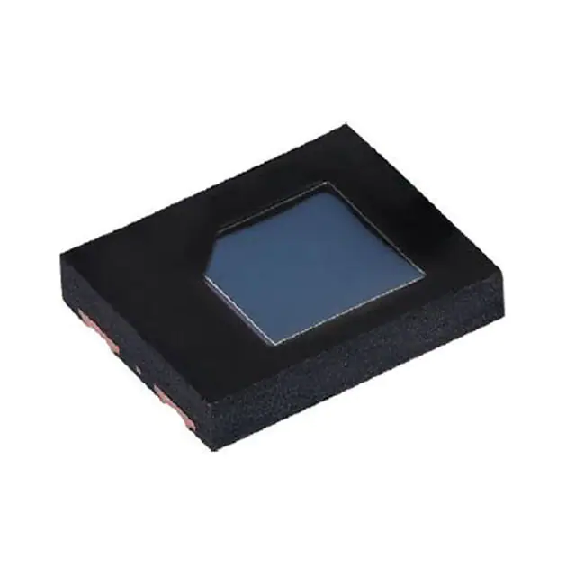
- Part No.:
- VEMD5080X01
- Manufacturer:
- Vishay Semiconductor Opto Division
- Category:
- Photodiodes
- Package:
- 4-SMD, No Lead Exposed Pad
- Datasheet:
-
VEMD5080X01.pdf
- Description:
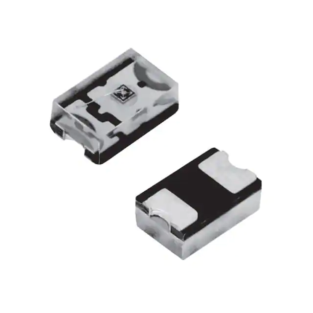
- SENSOR PHOTODIODE 950NM 4SMD
- Quantity:
- Payment:

- Shipping:

Inventory:2,231
Please send an inquiry. Send us your inquiry, and we will respond immediately.
Product details
Overview
VEMD5080X01 from Vishay Semiconductors is a silicon PIN photodiode optimized for high-speed, high-sensitivity detection of visible and near-infrared radiation (350–1100 nm), featuring a 7.5 mm² radiant sensitive area, ±65° half-sensitivity angle, and 45 μA reverse light current at 950 nm under 1 mW/cm² irradiance. It serves as a primary optical sensing element in compact, surface-mount photo-detection circuits operating from −40 °C to +110 °C.
For engineers reviewing the VEMD5080X01 datasheet, VEMD5080X01 pinout, VEMD5080X01 application, or VEMD5080X01 equivalent, key selection considerations include its AEC-Q101 qualification, 70 ns rise/fall time, low 0.6–10 nA dark current at 10 V reverse bias, 30–40 pF capacitance at 3 V reverse bias, and top-view SMD package with exposed cathode pad.
Technical Context
The VEMD5080X01 operates in photovoltaic or photoconductive mode with reverse bias up to 20 V, delivering fast transient response due to low junction capacitance and optimized PIN structure. Its spectral peak at 950 nm and broad 350–1100 nm bandwidth enable reliable detection across visible and NIR bands.
Thermal stability is supported by defined temperature coefficients: −3.0 mV/K for open-circuit voltage and +0.1 %/K for short-circuit current. The device's MSL 4 rating (72 h floor life) and Pb-free reflow compatibility per J-STD-020 ensure robust manufacturability in automotive and industrial SMT lines.
Key Specifications
| Parameter | Value and Actual Design Meaning |
|---|---|
| Reverse light current (950 nm) | 45 μA typical at 5 V reverse bias and 1 mW/cm² - defines signal output level for NIR sensing |
| Rise / fall time | 70 ns each at 10 V, 1 kΩ load, 830 nm - enables >5 MHz optical pulse detection |
| Diode capacitance | 30–40 pF at 3 V reverse bias - impacts AC bandwidth and noise coupling in transimpedance amplifiers |
| Angle of half sensitivity | ±65° - determines field-of-view acceptance for proximity or position sensing |
| Spectral range | 350–1100 nm - supports dual-band visible+NIR operation without filtering |
| Operating temperature | −40 °C to +110 °C - qualified for under-hood automotive and industrial ambient conditions |
| Reverse dark current | 0.6–10 nA at 10 V - sets lower limit of detectable irradiance in low-light applications |
Pinout & Package
Package: Top-view surface-mount device (SMD) in 5.0 × 4.0 × 0.9 mm outline with exposed cathode pad and tie bar electrically connected to cathode. Moisture sensitivity level (MSL) 4, floor life 72 h.
| Pin/Terminal | Circuit Role | Design Meaning |
|---|---|---|
| Anode | Positive terminal (P-side) | Connected to higher potential in reverse-biased operation; input to transimpedance amplifier in photoconductive mode |
| Cathode | Negative terminal (N-side) | Electrically tied to exposed pad and tie bar; common reference node and thermal path in PCB layout |
| NC | No connect | Non-functional metallization; must remain unconnected to avoid parasitic coupling or mechanical stress |
Key Features
| Feature | Design Value |
|---|---|
| AEC-Q101 qualification | Validated for automotive-grade reliability including temperature cycling, humidity testing, and ESD ≥2 kV HBM |
| Enhanced visible-light sensitivity | Delivers 5.0 μA Ira,G at 525 nm (green) under 0.2 mW/cm² - improves contrast detection in ambient-light environments |
| Low-profile SMD package | 0.9 mm height enables integration into space-constrained modules such as medical sensors and wearable devices |
| High radiant sensitive area | 7.5 mm² active area increases photon capture efficiency - reduces required optical gain and system power |
Applications
| Industrial Proximity Sensing | Automotive Occupancy Detection |
|---|---|
Use Scenario: Detecting presence of objects on conveyor belts or within automated assembly stations using modulated IR illumination. IC Role / Device Role / Timing Role: Primary photodetector converting reflected 950 nm pulses into proportional reverse current for timing-critical edge detection. Use Value: 70 ns response time enables sub-millisecond object localization; ±65° angular tolerance accommodates misalignment in factory-floor mounting. | Use Scenario: Monitoring seat occupancy via reflected NIR light in driver/passenger airbag control systems. IC Role / Device Role / Timing Role: AEC-Q101-qualified optical sensor providing fail-safe input to occupant classification ECU under wide temperature and vibration conditions. Use Value: Stable −40 °C to +110 °C operation ensures reliability in parked-car summer heat and cold-start winter conditions. |
| Hygienic Surface Monitoring | UV-Vis Spectrophotometer Channel |
Use Scenario: Non-contact detection of hand-washing completion or surface contamination in touchless dispensers and medical equipment. IC Role / Device Role / Timing Role: Visible-light-sensitive photodiode capturing green (525 nm) and blue (460 nm) reflectance signatures for color-based material discrimination. Use Value: 18 μA Ira,B at 460 nm and 5.0 μA Ira,G at 525 nm support multi-wavelength ratio analysis without external filters. | Use Scenario: Low-noise photodetection channel in portable spectrophotometers measuring absorbance across 350–1100 nm. IC Role / Device Role / Timing Role: Broadband photodiode generating calibrated photocurrent for analog-to-digital conversion of spectral intensity data. Use Value: 0.6–10 nA dark current at 25 °C enables high dynamic range (>80 dB) measurement of weak UV signals alongside strong NIR peaks. |
Equivalent & Alternatives
The following parts are listed as comparable options for similar photodiode applications.
| Alternative Part | Technical Difference | Application Difference | Selection Advice |
|---|---|---|---|
| VEMD5080X02 | Same package and spectral response, but rated for 30 V reverse voltage (vs. 20 V) and higher 350 mW power dissipation | Better suited for high-voltage biasing or higher irradiance environments where dark current headroom is critical | Select VEMD5080X02 when operating above 15 V reverse bias or requiring extended thermal margin beyond 215 mW |
| TEMD6200FX01 | Smaller 2.5 × 2.0 mm package, 1.2 mm² active area, 35 μA Ira at 950 nm, ±50° viewing angle | Optimized for ultra-compact designs with lower signal output and narrower FOV; not AEC-Q101 qualified | Choose TEMD6200FX01 only for space-constrained consumer electronics where automotive qualification is unnecessary |
Compared with VEMD5080X01, VEMD5080X02 offers higher reverse voltage and power handling for demanding bias conditions, while TEMD6200FX01 trades sensitivity and qualification for miniaturization - making VEMD5080X01 the balanced choice for automotive-grade, medium-FOV, high-signal NIR/visible detection.
Availability
VEMD5080X01 is available at Aetrix Electronics and suitable for industrial proximity sensing, automotive occupancy detection, hygienic surface monitoring, and UV-Vis spectrophotometer channel applications requiring stable component supply across production lifecycles.
Supply support for VEMD5080X01 includes scheduled delivery planning, volume procurement assistance, BOM continuity management, traceable sourcing, and lifecycle availability coordination for OEM customers, industrial embedded developers, connected-device designers, and electronics production programs.
Manufacturer
Vishay Intertechnology is a global manufacturer of discrete semiconductors and passive components, specializing in high-reliability optoelectronics, power management, and sensing solutions for automotive, industrial, and computing markets.
The VEMD5080X01 belongs to Vishay's high-speed silicon PIN photodiode product line, engineered specifically for AEC-Q101-compliant optical sensing in harsh environments where spectral breadth, angular consistency, and thermal stability are critical.
FAQ
What is the maximum reverse voltage rating for the VEMD5080X01?
The VEMD5080X01 has an absolute maximum reverse voltage rating of 20 V at 25 °C ambient temperature. Exceeding this value risks irreversible junction breakdown. Derating is required above 25 °C per the thermal resistance specification (RthJA = 350 K/W); for example, at 85 °C ambient, the safe continuous reverse bias drops to approximately 14 V to maintain junction temperature below 110 °C. Always refer to the Absolute Maximum Ratings table in the official VEMD5080X01 datasheet for full derating guidance.
Is the VEMD5080X01 suitable for photovoltaic (zero-bias) operation?
Yes, the VEMD5080X01 can operate in photovoltaic mode, delivering up to 320 mV open-circuit voltage at 950 nm and 1 mW/cm² irradiance. However, its primary design intent is photoconductive operation with reverse bias (typically 3–5 V) to achieve 70 ns response time and linear current output. In photovoltaic mode, response slows significantly due to increased junction capacitance and reduced carrier sweep-out efficiency - use VEMD5080X01 in reverse bias for timing-critical applications.
Does the VEMD5080X01 require external filtering for visible-light rejection?
No, the VEMD5080X01 does not require external filtering to reject visible light - it is explicitly enhanced for visible-light sensitivity, with measured reverse light currents of 5.0 μA at 525 nm and 18 μA at 460 nm. If visible-light rejection is needed (e.g., for pure NIR detection), an external bandpass or longpass filter must be added. The device's native 350–1100 nm spectral response makes it ideal for applications requiring broadband or multi-wavelength detection without filtering.
How is the cathode terminal identified on the VEMD5080X01 package?
The cathode terminal of the VEMD5080X01 is electrically connected to both the exposed metal pad on the bottom of the package and the tie bar located between the anode and NC terminals on the top side. The anode is the isolated top-side pad adjacent to the tie bar. This dual-cathode configuration provides low-inductance grounding and efficient thermal conduction - PCB layout must connect the exposed pad directly to ground plane to maintain specified thermal resistance (RthJA = 350 K/W) and ESD performance.
What is the moisture sensitivity level (MSL) and floor life of the VEMD5080X01?
The VEMD5080X01 is rated MSL 4 per J-STD-020, with a floor life of 72 hours at ambient conditions below 30 °C and 60 % relative humidity. After opening the moisture barrier bag, the device must be soldered within 72 hours or subjected to baking (e.g., 96 h at 60 °C, RH < 5 %) before reflow. Failure to comply risks popcorning or delamination during Pb-free reflow (peak 260 °C), as confirmed in the official VEMD5080X01 packaging documentation.
VEMD5080X01 Specifications
- Product attributes
- Attribute value
- Manufacturer:
- Vishay Semiconductor Opto Division
- Series:
- -
- Package/Case:
- 4-SMD, No Lead Exposed Pad
- Packaging:
- Tape & Reel (TR)
- Product Status:
- Active
- Wavelength:
- 950nm
- Color - Enhanced:
- -
- Spectral Range:
- 350nm ~ 1100nm
- Diode Type:
- PIN
- Responsivity @ nm:
- -
- Response Time:
- 70ns
- Voltage - DC Reverse (Vr) (Max):
- 20 V
- Current - Dark (Typ):
- -
- Active Area:
- 7.5mm²
- Viewing Angle:
- 65°
- Operating Temperature:
- -40°C ~ 110°C
- Grade:
- Automotive
- Qualification:
- AEC-Q101
- Mounting Type:
- Surface Mount
VEMD5080X01 FAQ
1.How can I place an order for VEMD5080X01 through Aetrix?
Please submit a Request for Quotation (RFQ) for VEMD5080X01 on Aetrix. Our sales agent will provide a competitive quotation and guide you through the order confirmation once you accept the terms.
2.Are the price and stock information for VEMD5080X01 reliable?
The price and inventory of VEMD5080X01 are updated periodically and may fluctuate due to market conditions. Stock and pricing data are typically refreshed every 24 hours. Quotation validity for VEMD5080X01 is usually 5 days.
3.What payment methods are accepted for VEMD5080X01?
We accept Wire Transfer, PayPal, Credit Card, Western Union, MoneyGram, and Escrow for VEMD5080X01 transactions.
Note: Certain payment methods may incur a processing fee.
4.How is shipping managed for VEMD5080X01?
VEMD5080X01 orders can be shipped via leading logistics carriers, including DHL, UPS, FedEx, TNT, or Registered Mail.
Once your VEMD5080X01 order is processed, you will receive an email with the shipment details and tracking number.
Note: Tracking information may take up to 24 hours to appear. Express delivery typically takes 3–5 business days.
5.How can I obtain technical support or documentation for VEMD5080X01?
For technical support, including VEMD5080X01 datasheets, pinout diagrams, or application guidance, please contact our engineering support team. They can provide detailed documentation and assistance for your VEMD5080X01 requirements.
6.How does Aetrix verify that VEMD5080X01 is sourced from the original manufacturer or authorized distributors?
All VEMD5080X01 products on Aetrix are procured from qualified distributors and authorized channels. Our dedicated quality assurance team conducts strict verification, including traceability checks and, if necessary, third-party testing. This ensures that VEMD5080X01 meets industry standards.
7.What is the process for return or replacement of VEMD5080X01?
All VEMD5080X01 units undergo pre-shipment inspection (PSI). If there is an issue with VEMD5080X01, returns or replacements are accepted under the following conditions:
1.Quantity discrepancies, incorrect items, or visible external defects (such as breakage or corrosion), acknowledged by Aetrix.
2.The issue is reported within 90 days of delivery.
3.The VEMD5080X01 part is unused and in its original packaging.
Return procedure for VEMD5080X01:
1.Submit a request within 90 days.
2.Obtain a Return Material Authorization (RMA) from Aetrix.
VEMD5080X01 Tags
-
OP999
TT Electronics/Optek Technology
-
TEMD6200FX01
Vishay Semiconductor Opto Division
-
SFH 203 FA
ams-OSRAM USA INC.
-
SFH 229FA
ams-OSRAM USA INC.
-
SFH 229
ams-OSRAM USA INC.
-
SFH 2704
ams-OSRAM USA INC.
-
VEMD2000X01
Vishay Semiconductor Opto Division
-
VEMD2020X01
Vishay Semiconductor Opto Division
-
VEMD2520X01
Vishay Semiconductor Opto Division
-
VEMD2023SLX01
Vishay Semiconductor Opto Division
-
VEMD2023X01
Vishay Semiconductor Opto Division
-
TEMD7000X01
Vishay Semiconductor Opto Division
Tech Hub

Comparator circuit design covering voltage thresholds, input limits, open-collector outputs, LM393 wiring, op-amp differences, hysteresis, timing, window detection and practical fault diagnosis.
Schmitt triggers use separate rising and falling thresholds to stabilize slow or noisy signals. This guide covers hysteresis, 74HC14 and 74HCT14 selection, comparator calculations, RC oscillators and p…
Counterfeit components can hide behind convincing markings and passing basic function tests. This engineering reference covers source traceability, external inspection, X-ray, XRF, electrical testing, …
A practical engineering and sourcing framework covering lifecycle verification, lifetime-buy calculations, replacement qualification, supplier checks and counterfeit-risk controls.
TTL and CMOS logic families differ in thresholds, loading, output drive, power and timing. This engineering guide compares 74HC and 74HCT, calculates noise margins and checks 3.3 V/5 V compatibility.
A practical engineering guide to 3.3V and 5V logic compatibility, input thresholds, resistor dividers, translator ICs, MOSFET level shifting, I2C pull-ups, timing limits and power-sequencing risks.
The 74HC595 uses push-pull logic outputs, while the TPIC6B595 uses 50 V open-drain DMOS sinks for higher-power loads. This guide compares timing, current limits, 3.3 V interfacing, load wiring, thermal…
The 74HC595 converts serial data into eight stable parallel outputs. This guide covers pin functions, shift and storage timing, OE and MR behavior, drive-current limits, cascading, voltage compatibilit…
A technical comparison of level-sensitive latches and edge-triggered flip-flops, covering timing windows, setup and hold limits, master–slave operation, time borrowing, race-through, HDL inference and…
A D latch stores one bit while Enable controls when data can pass. This reference covers gate-level operation, truth tables, transparency, setup and hold timing, LE versus OE, common ICs and practical …









