Vishay Semiconductor Opto Division VLMY3100-GS08
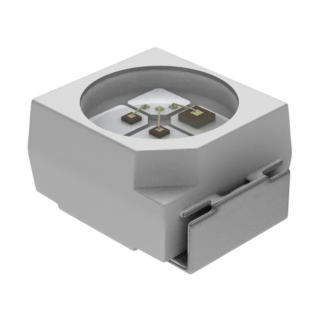
- Part No.:
- VLMY3100-GS08
- Manufacturer:
- Vishay Semiconductor Opto Division
- Category:
- LED Indication - Discrete
- Package:
- 2-SMD, J-Lead
- Datasheet:
-
VLMY3100-GS08.pdf
- Description:
- LED YELLOW CLEAR 2PLCC SMD
- Quantity:
- Payment:

- Shipping:

Inventory:10,274
Please send an inquiry. Send us your inquiry, and we will respond immediately.
Product details
Overview
VLMY3100-GS08 from Vishay Semiconductors is a surface-mount yellow LED in PLCC-2 package, with dominant wavelength 581–594 nm, luminous intensity 2.8–11 mcd at 10 mA, forward voltage 2.1–2.8 V at 20 mA, and ±60° viewing angle - used for indicator and backlighting in office equipment and LCD panels.
For engineers reviewing the VLMY3100-GS08 datasheet, VLMY3100-GS08 pinout, VLMY3100-GS08 application, or VLMY3100-GS08 equivalent, this page delivers verified optical, electrical, thermal, and packaging data - including JEDEC level 2a preconditioning compliance, 8 mm tape packaging, and PLCC-2 mechanical dimensions - to support SMT placement, reflow soldering, and brightness-binned design validation.
Technical Context
The VLMY3100-GS08 is a GaAsP-on-GaP yellow LED optimized for high-brightness indicator and backlight functions in compact SMD layouts. It operates at 10 mA test current for photometric characterization and supports 20 mA DC forward current with thermal resistance of 400 K/W when mounted on ≥16 mm² PCB pad.
Its non-diffused lens enables efficient coupling to light pipes and flat backlight assemblies, while its ±60° half-intensity angle ensures wide visibility without excessive lateral spread. The device meets CECC 00802 and J-STD-020 for infrared, vapor-phase, and wave soldering processes.
Key Specifications
| Parameter | Value and Actual Design Meaning |
|---|---|
| Dominant wavelength | 581–594 nm - defines visible yellow output suitable for status indication where color differentiation from red/green is critical |
| Luminous intensity | 2.8–11 mcd at 10 mA - brightness binned per reel (IVmax/IVmin ≤ 1.6), enabling consistent visual performance across production units |
| Forward voltage | 2.1–2.8 V at 20 mA - low power consumption compatible with 3.3 V and 5 V logic-supplied LED drivers |
| Viewing angle | ±60° - wide angular distribution ideal for front-panel indicators and uniform edge-lit backlighting |
| Absolute max current | 20 mA DC - sets maximum continuous drive level for thermal reliability at Tamb ≤ 74 °C |
| Junction temperature | 100 °C - defines upper thermal limit for sustained operation; requires RthJA = 400 K/W PCB layout for safe derating |
| Reverse voltage | 6 V - limits reverse bias exposure during circuit transients or multiplexed driving schemes |
Pinout & Package
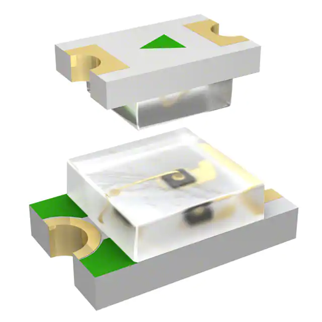
Package: PLCC-2 (Plastic Leaded Chip Carrier, 2-terminal), low-profile SMD with white thermoplastic body, clear epoxy lens, and embedded lead frame. Dimensions: 3.5 ± 0.2 mm × 2.8 ± 0.15 mm × 1.75 ± 0.1 mm (L × W × H); mounting pad layout defined per drawing 6.541-5067.01-4.
| Pin/Terminal | Circuit Role | Design Meaning |
|---|---|---|
| Anode (A) | Positive terminal | Connected to current source or driver high-side; polarity must be observed to avoid reverse breakdown |
| Cathode (K) | Negative terminal | Connected to ground or driver low-side; marked by notch or chamfer on package top surface |
Key Features
| Feature | Design Value |
|---|---|
| Non-diffused lens | Enables precise optical coupling into light guides and backlights without scattering loss |
| Luminous intensity ratio control | IVmax/IVmin ≤ 1.6 per reel - ensures minimal brightness variation across assembled units |
| JEDEC level 2a preconditioning | Validates moisture sensitivity handling prior to reflow, reducing popcorning risk during assembly |
| EIA/ICE standard package | Ensures compatibility with automated pick-and-place equipment and industry-standard tape feeders |
| Low power consumption | 2.1–2.8 V @ 20 mA enables direct drive from microcontroller GPIOs or low-dropout LED drivers |
Applications
| Office Equipment Indicator | Audio/Video Backlight |
|---|---|
Use Scenario: Status indication on printers, scanners, and multifunction devices requiring high-visibility yellow feedback under ambient lighting. IC Role / Device Role / Timing Role: Standalone optical output device driven by microcontroller GPIO or dedicated LED driver IC. Use Value: Consistent 581–594 nm yellow output ensures color-coded status recognition distinct from green OK/red error signals. |
Use Scenario: Edge-lit backlight for front-panel buttons and displays in AV receivers and streaming devices. IC Role / Device Role / Timing Role: Light source coupled to light pipe or diffuser film; no timing or signal conditioning required. Use Value: ±60° viewing angle provides uniform illumination across narrow bezels without hotspots or dark zones. |
| LCD Symbol Backlight | Telecom Device Indicator |
Use Scenario: Illumination of segmented symbols (e.g., "LINE", "HOLD", "MUTE") on monochrome LCD modules in industrial HMIs. IC Role / Device Role / Timing Role: DC-driven discrete emitter; brightness controlled via PWM or constant-current source. Use Value: Non-diffused lens maximizes light transfer efficiency into small-aperture LCD cutouts, improving contrast ratio. |
Use Scenario: Call status and line activity indicators in VoIP phones and fax machines operating in mixed-light environments. IC Role / Device Role / Timing Role: Visual signaling element powered from system 3.3 V rail with series resistor or current-regulated driver. Use Value: 2.8–11 mcd output at 10 mA ensures legibility at >2 m distance while maintaining low power draw. |
Equivalent & Alternatives
The following parts are listed as comparable options for similar yellow LED indicator applications.
| Alternative Part | Technical Difference | Application Difference | Selection Advice |
|---|---|---|---|
| VLMY3101-GS08 | Higher typical luminous intensity (10 mcd vs. 11 mcd) and tighter binning (4.5–11.2 mcd range) | Better suited for applications requiring higher brightness consistency across units | Select when tighter IV tolerance and higher minimum output are needed without changing footprint or drive conditions |
| LYT670J1L2 (OSRAM) | Same PLCC-2 package, 585 nm peak wavelength, 2.2–2.8 V VF, but wider IV range (3–12 mcd at 10 mA) | Compatible for general-purpose yellow indication but lacks VLMY3100-GS08's IV ratio control (≤1.6) | Choose for cost-sensitive designs where absolute brightness matching is less critical than form-fit-function replacement |
Compared with VLMY3100-GS08, VLMY3101-GS08 offers higher baseline intensity and tighter binning for improved visual uniformity, while LYT670J1L2 provides cross-manufacturer sourcing flexibility at the expense of luminous intensity consistency per reel.
Availability
VLMY3100-GS08 is available at Aetrix Electronics and suitable for office equipment indicators, audio/video backlighting, LCD symbol illumination, and telecom device status signaling requiring stable component supply, brightness-consistent reels, and JEDEC-compliant moisture handling.
Supply support for VLMY3100-GS08 includes scheduled delivery planning, volume procurement assistance, BOM continuity management, traceable sourcing, and lifecycle availability coordination for OEM customers, industrial embedded developers, connected-device designers, and electronics production programs.
Manufacturer
Vishay Semiconductors is a global leader in discrete semiconductors and passive components, specializing in high-reliability optoelectronics, power MOSFETs, diodes, and resistive sensors.
The VLMY3100-GS08 belongs to Vishay's VLM.310. standard SMD LED family, designed specifically for high-volume, automated assembly of visual indicators and backlighting in consumer, office, and telecom equipment.
FAQ
What is the dominant wavelength range of the VLMY3100-GS08?
The VLMY3100-GS08 has a dominant wavelength range of 581–594 nm, measured at 10 mA forward current. This places its output firmly in the yellow portion of the visible spectrum, distinct from orange-red (612–625 nm) and green (562–575 nm) variants in the same VLM.310. family. The value is confirmed in the Optical and Electrical Characteristics table on page 3 of Vishay document 84789.
What is the maximum DC forward current rating for VLMY3100-GS08?
The VLMY3100-GS08 is rated for a maximum DC forward current of 20 mA at ambient temperatures ≤ 74 °C. Exceeding this current without thermal derating risks exceeding the 100 °C junction temperature limit. Absolute maximum ratings are specified in the "Absolute Maximum Ratings" table on page 2 of Vishay document 84789.
Does VLMY3100-GS08 have a diffused or non-diffused lens?
The VLMY3100-GS08 features a non-diffused lens, explicitly stated in the FEATURES section on page 1 of Vishay document 84789. This design enhances coupling efficiency into light pipes and edge-lit backlight structures, minimizing lateral light scatter and maximizing directional output.
What tape option does VLMY3100-GS08 use, and how many units are on the reel?
VLMY3100-GS08 ships in GS08 tape configuration: an antistatic 8 mm blister tape containing 1500 pieces per reel. This is confirmed in the "METHOD OF TAPING" section and Figure 25 (Reel Dimensions – GS08) on page 10 of Vishay document 84789.
Is VLMY3100-GS08 compatible with lead-free reflow soldering?
Yes, VLMY3100-GS08 is qualified for lead-free reflow soldering per J-STD-020, with a peak package body temperature limit of 260 °C for ≤ 10 seconds. The recommended profile is shown in Figure 27 (Vishay Lead-free Reflow Soldering Profile) on page 10 of Vishay document 84789.
VLMY3100-GS08 Specifications
- Product attributes
- Attribute value
- Manufacturer:
- Vishay Semiconductor Opto Division
- Series:
- VLM.3
- Package/Case:
- 2-SMD, J-Lead
- Packaging:
- Tape & Reel (TR)
- Product Status:
- Active
- Color:
- Yellow
- Configuration:
- Standard
- Lens Color:
- -
- Lens Transparency:
- Clear
- Millicandela Rating:
- 10mcd
- Lens Style:
- Round with Flat Top
- Lens Size:
- 2.40mm Dia
- Voltage - Forward (Vf) (Typ):
- 2.1V
- Current - Test:
- 10mA
- Viewing Angle:
- 120°
- Mounting Type:
- Surface Mount
- Wavelength - Dominant:
- 588nm
- Wavelength - Peak:
- 585nm
- Features:
- -
- Grade:
- -
- Qualification:
- -
- Supplier Device Package:
- 2-PLCC
- Size / Dimension:
- 3.00mm L x 2.80mm W
VLMY3100-GS08 FAQ
1.How can I place an order for VLMY3100-GS08 through Aetrix?
Please submit a Request for Quotation (RFQ) for VLMY3100-GS08 on Aetrix. Our sales agent will provide a competitive quotation and guide you through the order confirmation once you accept the terms.
2.Are the price and stock information for VLMY3100-GS08 reliable?
The price and inventory of VLMY3100-GS08 are updated periodically and may fluctuate due to market conditions. Stock and pricing data are typically refreshed every 24 hours. Quotation validity for VLMY3100-GS08 is usually 5 days.
3.What payment methods are accepted for VLMY3100-GS08?
We accept Wire Transfer, PayPal, Credit Card, Western Union, MoneyGram, and Escrow for VLMY3100-GS08 transactions.
Note: Certain payment methods may incur a processing fee.
4.How is shipping managed for VLMY3100-GS08?
VLMY3100-GS08 orders can be shipped via leading logistics carriers, including DHL, UPS, FedEx, TNT, or Registered Mail.
Once your VLMY3100-GS08 order is processed, you will receive an email with the shipment details and tracking number.
Note: Tracking information may take up to 24 hours to appear. Express delivery typically takes 3–5 business days.
5.How can I obtain technical support or documentation for VLMY3100-GS08?
For technical support, including VLMY3100-GS08 datasheets, pinout diagrams, or application guidance, please contact our engineering support team. They can provide detailed documentation and assistance for your VLMY3100-GS08 requirements.
6.How does Aetrix verify that VLMY3100-GS08 is sourced from the original manufacturer or authorized distributors?
All VLMY3100-GS08 products on Aetrix are procured from qualified distributors and authorized channels. Our dedicated quality assurance team conducts strict verification, including traceability checks and, if necessary, third-party testing. This ensures that VLMY3100-GS08 meets industry standards.
7.What is the process for return or replacement of VLMY3100-GS08?
All VLMY3100-GS08 units undergo pre-shipment inspection (PSI). If there is an issue with VLMY3100-GS08, returns or replacements are accepted under the following conditions:
1.Quantity discrepancies, incorrect items, or visible external defects (such as breakage or corrosion), acknowledged by Aetrix.
2.The issue is reported within 90 days of delivery.
3.The VLMY3100-GS08 part is unused and in its original packaging.
Return procedure for VLMY3100-GS08:
1.Submit a request within 90 days.
2.Obtain a Return Material Authorization (RMA) from Aetrix.
VLMY3100-GS08 Tags

-
LTST-C281KRKT
Lite-On Inc.
-
150060GS75000
Würth Elektronik

-
150060VS75000
Würth Elektronik

-
150060AS75000
Würth Elektronik

-
150060YS75000
Würth Elektronik

-
150060SS75000
Würth Elektronik

-
150060BS75000
Würth Elektronik
-
151031VS06000
Würth Elektronik
-
151033RS03000
Würth Elektronik
-
150080BS75000
Würth Elektronik
-
150080GS75000
Würth Elektronik
-
150141GS73100
Würth Elektronik
Tech Hub

Comparator circuit design covering voltage thresholds, input limits, open-collector outputs, LM393 wiring, op-amp differences, hysteresis, timing, window detection and practical fault diagnosis.
Schmitt triggers use separate rising and falling thresholds to stabilize slow or noisy signals. This guide covers hysteresis, 74HC14 and 74HCT14 selection, comparator calculations, RC oscillators and p…
Counterfeit components can hide behind convincing markings and passing basic function tests. This engineering reference covers source traceability, external inspection, X-ray, XRF, electrical testing, …
A practical engineering and sourcing framework covering lifecycle verification, lifetime-buy calculations, replacement qualification, supplier checks and counterfeit-risk controls.
TTL and CMOS logic families differ in thresholds, loading, output drive, power and timing. This engineering guide compares 74HC and 74HCT, calculates noise margins and checks 3.3 V/5 V compatibility.
A practical engineering guide to 3.3V and 5V logic compatibility, input thresholds, resistor dividers, translator ICs, MOSFET level shifting, I2C pull-ups, timing limits and power-sequencing risks.
The 74HC595 uses push-pull logic outputs, while the TPIC6B595 uses 50 V open-drain DMOS sinks for higher-power loads. This guide compares timing, current limits, 3.3 V interfacing, load wiring, thermal…
The 74HC595 converts serial data into eight stable parallel outputs. This guide covers pin functions, shift and storage timing, OE and MR behavior, drive-current limits, cascading, voltage compatibilit…
A technical comparison of level-sensitive latches and edge-triggered flip-flops, covering timing windows, setup and hold limits, master–slave operation, time borrowing, race-through, HDL inference and…
A D latch stores one bit while Enable controls when data can pass. This reference covers gate-level operation, truth tables, transparency, setup and hold timing, LE versus OE, common ICs and practical …










