
 My Inquiry
 My Account


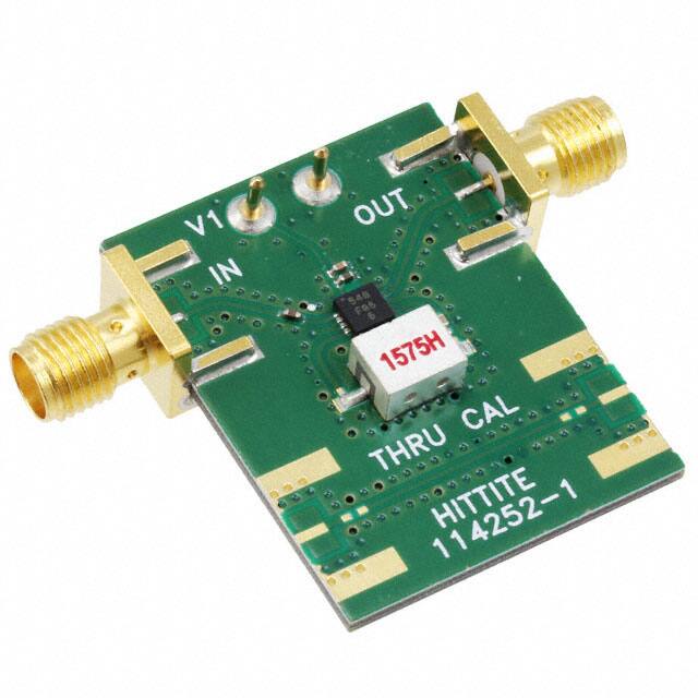
Analog Devices Inc. 114254-HMC548LP3
- Part No.:
- 114254-HMC548LP3
- Manufacturer:
- Analog Devices Inc.
- Category:
- RF, RFID, Wireless Evaluation Boards
- Package:
- Datasheet:
-
 114254-HMC548LP3.pdf
- Description:
- BOARD EVAL HMC548LP3E 1575MHZ
- Quantity:
- Payment:

- Shipping:

Inventory:4,052
Please send an inquiry. Send us your inquiry, and we will respond immediately.
Product details
Overview
HMC548LP3 from Hittite Microwave Corporation (now part of Analog Devices) is a dual-stage SiGe HBT MMIC low-noise amplifier optimized for 1.2–3.0 GHz RF front-ends. It delivers 23 dB typical gain, 1.3 dB noise figure, and +21 dBm output IP3 at +5 V supply, with interstage access (pins 4 and 9) enabling external bandpass filtering - critical for GPS L1 (1575 MHz) receiver pre-amplification in antenna modules.
For engineers reviewing the HMC548LP3 datasheet, HMC548LP3 pinout, HMC548LP3 application, or HMC548LP3 equivalent, key selection criteria include its two-stage architecture with filter insertion capability, 3×3 mm leadless SMT package, DC-coupled input stages requiring external blocking capacitors, and validated performance across –40°C to +85°C operating range.
Technical Context
The HMC548LP3 integrates two internally matched SiGe HBT amplifier stages in a single die, with dedicated RFIN1/RFOUT1 and RFIN2/RFOUT2 signal paths separated by an accessible interstage node. This topology enables placement of an external bandpass filter (e.g., 1575 MHz GPS L1) between pins 4 (RFOUT1) and 9 (RFIN2), preserving low noise figure while rejecting out-of-band blockers.
It operates from a single +3 to +5 V supply, draws 10–21 mA depending on Vcc, and requires external bypassing (1000 pF and 18,000 pF) on Vcc (pin 15). All ground pins (2,3,5–8,10,11,13,14,16) and the exposed paddle must be soldered to RF/DC ground per RF layout best practices.
Key Specifications
| Parameter | Value and Actual Design Meaning |
|---|---|
| Frequency Range | 1.2–3.0 GHz operating bandwidth; supports GPS L1 (1575 MHz) with external filter. |
| Gain | 23 dB typical at 1575 MHz; enables high-sensitivity receiver front-end amplification. |
| Noise Figure | 1.3 dB typical at 1575 MHz; ensures minimal degradation of system noise floor. |
| Output IP3 | +21 dBm typical; provides strong linearity against adjacent-channel interferers. |
| P1dB | +11 dBm typical; defines usable dynamic range before compression onset. |
| Supply Voltage | +3 to +5 V DC; single-supply operation simplifies biasing in portable and embedded systems. |
| Operating Temp | –40°C to +85°C; qualified for automotive telematics and industrial GNSS applications. |
Pinout & Package
Package: 3×3 mm leadless surface-mount package (MSL1, Sn/Pb finish); exposed ground paddle requires soldering to PCB RF ground plane.
| Pin/Terminal | Circuit Role | Design Meaning |
|---|---|---|
| 1 | RFIN1 | DC-coupled 50 Ω RF input (1.2–2.0 GHz); requires external blocking capacitor. |
| 2,3,5–8,10,11,13,14,16 | GND | RF/DC ground connections; all must be soldered to minimize parasitic inductance. |
| 4 | RFOUT1 | AC-coupled 50 Ω RF output (1.2–2.0 GHz); connects to external filter input. |
| 9 | RFIN2 | DC-coupled 50 Ω RF input (1.2–2.0 GHz); accepts filtered signal from pin 4. |
| 12 | RFOUT2 | AC-coupled 50 Ω final RF output; matches standard 50 Ω system interface. |
| 15 | Vcc | +3 to +5 V power supply; requires 1000 pF and 18,000 pF bypass capacitors. |
Key Features
| Feature | Design Value |
|---|---|
| Interstage Filter Access | Direct connection between RFOUT1 (pin 4) and RFIN2 (pin 9) enables insertion of external bandpass filters without degrading noise figure. |
| No External Matching Required | Internally matched 50 Ω inputs/outputs reduce design complexity and board space in GPS and navigation modules. |
| Low Noise Figure | 1.3 dB typical at GPS L1 frequency ensures maximum receiver sensitivity in weak-signal environments. |
| High Linearity | +21 dBm OIP3 and +11 dBm P1dB support robust operation in spectrally crowded bands (e.g., near cellular transmitters). |
| Single-Supply Operation | +3 to +5 V operation simplifies power architecture and enables compatibility with common embedded voltage rails. |
Applications
| GPS Antenna Modules | Automotive Telematics |
|---|---|
|
Use Scenario: Boosting weak satellite signals in compact GPS antenna assemblies mounted on vehicle roofs or dashboards. IC Role / Device Role / Timing Role: Receiver pre-amplifier placed immediately after antenna feed, preceding SAW filter and downconversion stage. Use Value: 1.3 dB noise figure preserves signal-to-noise ratio; interstage filter access rejects cellular 3G/4G interference without added loss. |
Use Scenario: Enabling real-time location tracking and emergency call (eCall) functionality in connected vehicles. IC Role / Device Role / Timing Role: Front-end LNA in multi-constellation GNSS receivers (GPS, GLONASS, Galileo) integrated into telematics control units. Use Value: –40°C to +85°C operation ensures reliability across automotive temperature extremes; dual-stage gain supports cascaded receiver architectures. |
| Location-Based Portables | Satellite Navigation Receivers |
|
Use Scenario: Enhancing position accuracy in handheld devices such as survey-grade RTK receivers and asset trackers. IC Role / Device Role / Timing Role: Low-noise amplification stage in battery-powered GNSS front-ends where power efficiency and sensitivity are critical. Use Value: 21 mA typical supply current at +5 V balances performance and battery life; 3×3 mm footprint minimizes PCB area. |
Use Scenario: High-precision navigation in marine, aviation, and UAV guidance systems requiring stable RF gain and phase response. IC Role / Device Role / Timing Role: Primary LNA in wideband (1.2–3.0 GHz) receiver chains supporting multiple GNSS bands and augmentation signals. Use Value: Validated broadband performance (gain flatness ±1.5 dB, NF <1.9 dB) ensures consistent behavior across frequency bands without recalibration. |
Equivalent & Alternatives
The following parts are listed as comparable options for similar low-noise amplifier applications.
| Alternative Part | Technical Difference | Application Difference | Selection Advice |
|---|---|---|---|
| HMC548LP3E | RoHS-compliant version with 100% matte tin lead finish and MSL1 rating up to 260°C peak reflow. | Identical RF performance and pinout; selected when lead-free assembly or higher reflow tolerance is required. | Drop-in replacement for HMC548LP3 in RoHS-compliant manufacturing flows. |
| QPL9057 | Single-stage GaAs pHEMT LNA; 0.65 dB NF at 1575 MHz, +19.5 dBm OIP3, 16 dB gain; 2×2 mm DFN package. | Lacks interstage filter access; suited for space-constrained designs where external filtering is handled upstream/downstream. | Preferred when minimal board area and ultra-low noise dominate over blocker rejection flexibility. |
Compared with HMC548LP3E, the HMC548LP3 offers identical RF specs but uses Sn/Pb finish and lower reflow ceiling (235°C); versus QPL9057, it trades slightly higher NF for superior interstage filtering capability and higher gain-making it optimal for GPS L1 systems facing strong out-of-band interferers.
Availability
HMC548LP3 is available at Aetrix Electronics and suitable for GPS antenna modules, automotive telematics units, and location-based portable electronics requiring stable component supply and long-term obsolescence management.
Supply support for HMC548LP3 includes scheduled delivery planning, volume procurement assistance, BOM continuity management, traceable sourcing, and lifecycle availability coordination for OEM customers, industrial embedded developers, connected-device designers, and electronics production programs.
Manufacturer
Hittite Microwave Corporation, acquired by Analog Devices in 2014, specialized in high-performance RF/microwave ICs for defense, aerospace, and communications markets.
The HMC548LP3 belongs to Hittite's SiGe HBT MMIC amplifier product line, designed specifically for high-linearity, low-noise front-end applications in GNSS, wireless infrastructure, and electronic warfare systems.
FAQ
What is the recommended external filter for HMC548LP3 in GPS L1 applications?
The HMC548LP3 datasheet specifies use of a 1.57–1.6 GHz bandpass filter (e.g., Amotech AMOBP1575P02-A1) between pins 4 (RFOUT1) and 9 (RFIN2). This filter provides ~2.5 dB insertion loss at 1575 MHz and enables effective rejection of nearby cellular and 3G signals without increasing system noise figure - a key advantage over pre-filtering approaches.
Does HMC548LP3 require external matching components?
No - the HMC548LP3 is internally matched to 50 Ω at both input and output ports across 1.2–2.0 GHz. However, external DC-blocking capacitors are required on RFIN1 (pin 1) and RFIN2 (pin 9), and bypass capacitors (1000 pF and 18,000 pF) must be placed on Vcc (pin 15) per the evaluation board layout guidelines.
What is the thermal resistance and maximum junction temperature for HMC548LP3?
The HMC548LP3 has a thermal resistance of 69 °C/W (junction to ground paddle) and a maximum junction temperature of 150 °C. At 85 °C case temperature, its continuous power dissipation is 0.942 W, derating linearly by 14 mW/°C above that point - critical for thermal design in sealed automotive enclosures.
Can HMC548LP3 operate from a +3 V supply, and how does performance change vs. +5 V?
Yes - the HMC548LP3 operates from +3 to +5 V. At +3 V, typical supply current drops to 10 mA (vs. 21 mA at +5 V), gain decreases by ~3 dB, and noise figure increases slightly (to 1.6 dB typ). The device remains fully functional across this range, enabling power-sensitive portable designs.
Is HMC548LP3 obsolete, and what is its lifecycle status?
While the original Hittite documentation marks HMC548LP3 as "OBSOLETE", Analog Devices continues to list it as active and available through authorized distributors. Aetrix Electronics maintains inventory and supports long-term supply for legacy designs, including full traceability and lifecycle coordination for industrial and automotive customers using HMC548LP3.
114254-HMC548LP3 Specifications
- Product attributes
- Attribute value
- Manufacturer:
- Analog Devices Inc.
- Series:
- -
- Packaging:
- Box
- Product Status:
- Obsolete
- Type:
- Amplifier
- Frequency:
- 1.575GHz
- Contents:
- Board(s)
- Utilized IC / Part:
- HMC548LP3
114254-HMC548LP3 FAQ
1.How can I place an order for 114254-HMC548LP3 through Aetrix?
Please submit a Request for Quotation (RFQ) for 114254-HMC548LP3 on Aetrix. Our sales agent will provide a competitive quotation and guide you through the order confirmation once you accept the terms.
2.Are the price and stock information for 114254-HMC548LP3 reliable?
The price and inventory of 114254-HMC548LP3 are updated periodically and may fluctuate due to market conditions. Stock and pricing data are typically refreshed every 24 hours. Quotation validity for 114254-HMC548LP3 is usually 5 days.
3.What payment methods are accepted for 114254-HMC548LP3?
We accept Wire Transfer, PayPal, Credit Card, Western Union, MoneyGram, and Escrow for 114254-HMC548LP3 transactions.
Note: Certain payment methods may incur a processing fee.
4.How is shipping managed for 114254-HMC548LP3?
114254-HMC548LP3 orders can be shipped via leading logistics carriers, including DHL, UPS, FedEx, TNT, or Registered Mail.
Once your 114254-HMC548LP3 order is processed, you will receive an email with the shipment details and tracking number.
Note: Tracking information may take up to 24 hours to appear. Express delivery typically takes 3–5 business days.
5.How can I obtain technical support or documentation for 114254-HMC548LP3?
For technical support, including 114254-HMC548LP3 datasheets, pinout diagrams, or application guidance, please contact our engineering support team. They can provide detailed documentation and assistance for your 114254-HMC548LP3 requirements.
6.How does Aetrix verify that 114254-HMC548LP3 is sourced from the original manufacturer or authorized distributors?
All 114254-HMC548LP3 products on Aetrix are procured from qualified distributors and authorized channels. Our dedicated quality assurance team conducts strict verification, including traceability checks and, if necessary, third-party testing. This ensures that 114254-HMC548LP3 meets industry standards.
7.What is the process for return or replacement of 114254-HMC548LP3?
All 114254-HMC548LP3 units undergo pre-shipment inspection (PSI). If there is an issue with 114254-HMC548LP3, returns or replacements are accepted under the following conditions:
1.Quantity discrepancies, incorrect items, or visible external defects (such as breakage or corrosion), acknowledged by Aetrix.
2.The issue is reported within 90 days of delivery.
3.The 114254-HMC548LP3 part is unused and in its original packaging.
Return procedure for 114254-HMC548LP3:
1.Submit a request within 90 days.
2.Obtain a Return Material Authorization (RMA) from Aetrix.
114254-HMC548LP3 Tags
-
113991054
Seeed Technology Co., Ltd
-
SC0918
Raspberry Pi

-
113991114
Seeed Technology Co., Ltd
-
ESP32-C6-DEVKITM-1-N4
Espressif Systems
-
ESP32-DEVKITM-1
Espressif Systems
-
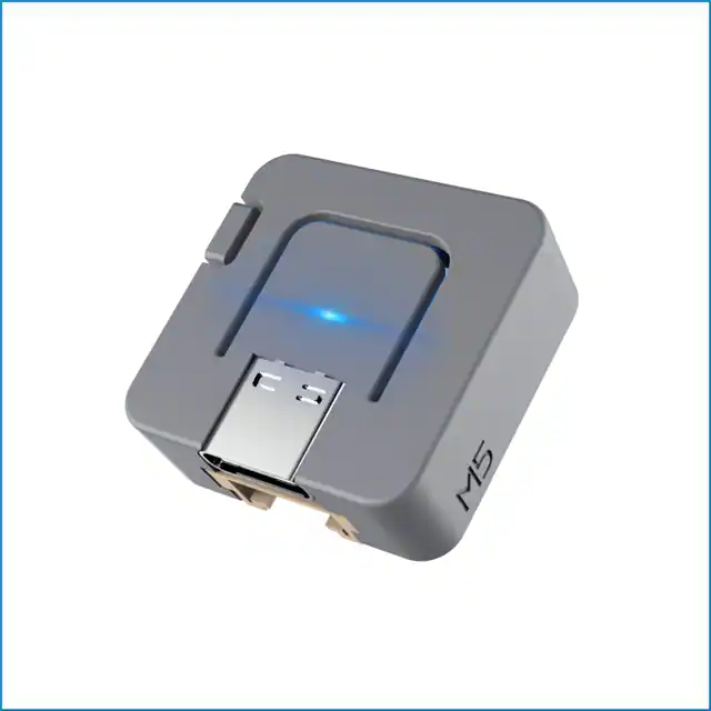
C008
M5Stack Technology Co., Ltd.
-
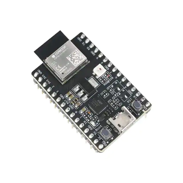
ESP32-C3-DEVKITC-02
Espressif Systems
-
ESP32-C6-DEVKITC-1-N8
Espressif Systems
-
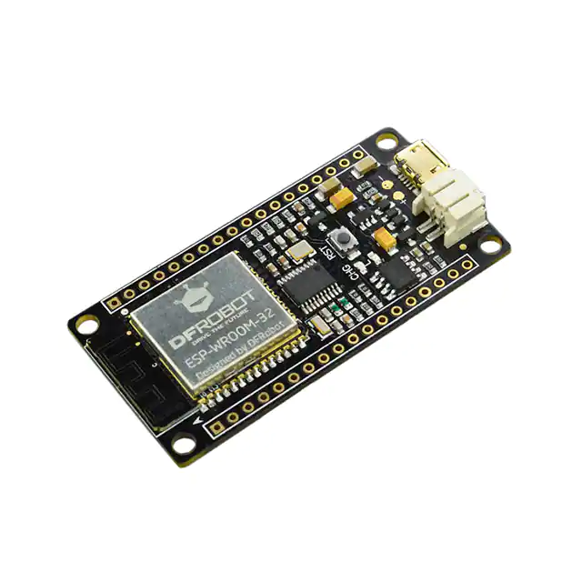
DFR0478
DFRobot
-
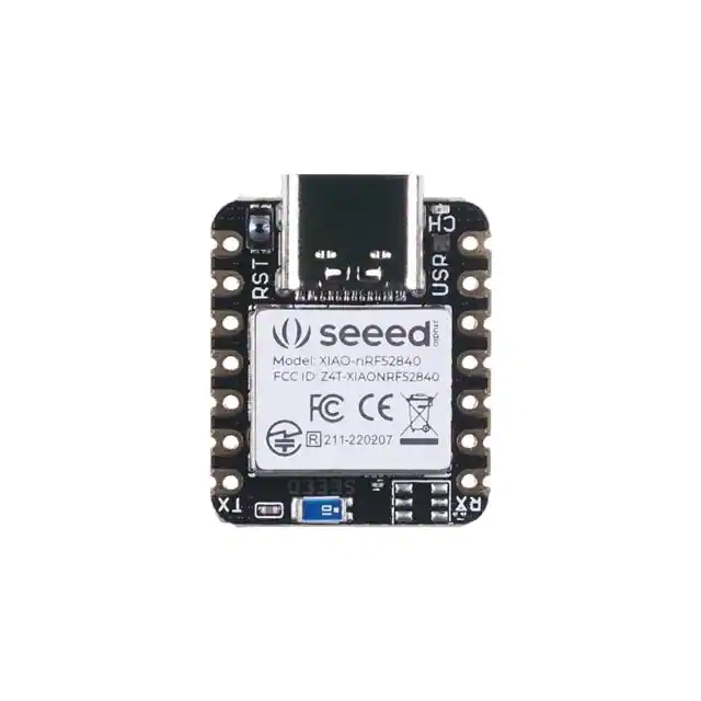
102010448
Seeed Technology Co., Ltd
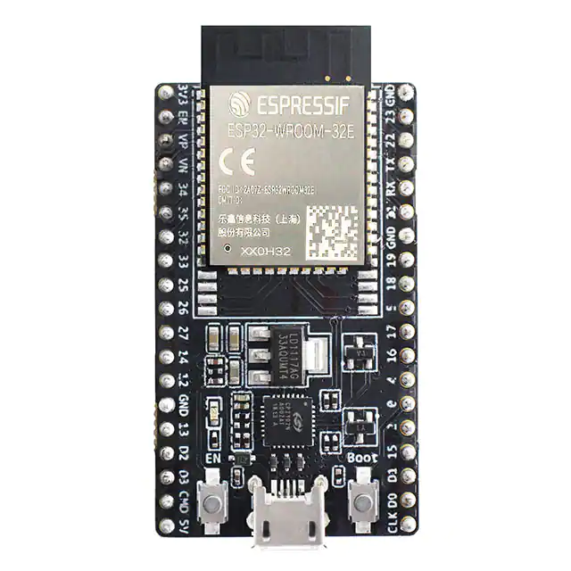
-
ESP32-DEVKITC-32E
Espressif Systems
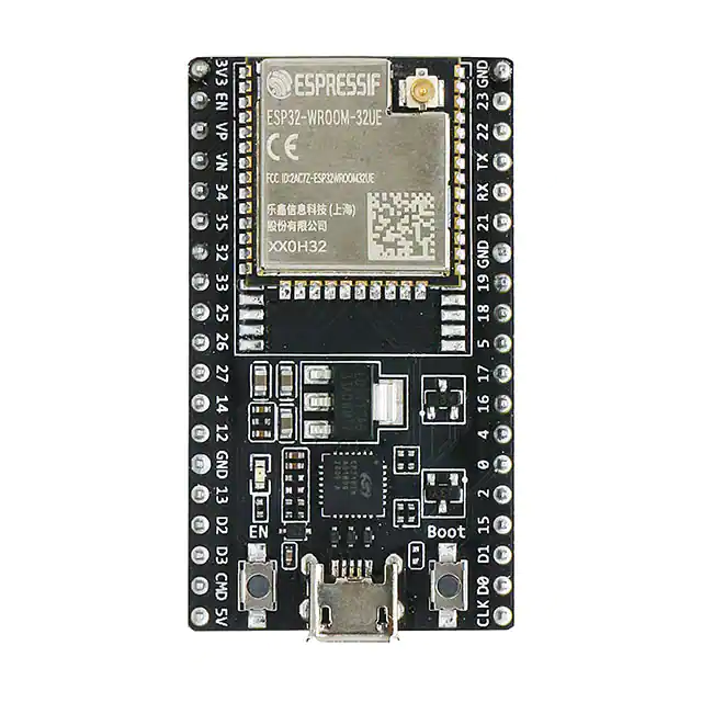
-
ESP32-DEVKITC-32UE
Espressif Systems
Tech Hub

A practical engineering guide to 3.3V and 5V logic compatibility, input thresholds, resistor dividers, translator ICs, MOSFET level shifting, I2C pull-ups, timing limits and power-sequencing risks.

The 74HC595 uses push-pull logic outputs, while the TPIC6B595 uses 50 V open-drain DMOS sinks for higher-power loads. This guide compares timing, current limits, 3.3 V interfacing, load wiring, thermal…

The 74HC595 converts serial data into eight stable parallel outputs. This guide covers pin functions, shift and storage timing, OE and MR behavior, drive-current limits, cascading, voltage compatibilit…

A technical comparison of level-sensitive latches and edge-triggered flip-flops, covering timing windows, setup and hold limits, master–slave operation, time borrowing, race-through, HDL inference and…

A D latch stores one bit while Enable controls when data can pass. This reference covers gate-level operation, truth tables, transparency, setup and hold timing, LE versus OE, common ICs and practical …

An SR latch stores one bit through cross-coupled feedback. This engineering reference covers NOR and NAND implementations, truth tables, forbidden-state recovery, gated operation, switch debouncing, fa…

Latch circuits retain one bit through feedback. This technical reference covers SR and D latches, truth tables, transparency, timing limits, latch-versus-flip-flop behavior, applications and common log…

An engineering guide to LED driver operation, constant-current and constant-voltage outputs, linear and switching topologies, dimming, IC selection, calculations, replacement compatibility, and fault c…

Operational amplifier guide covering op amp basics, feedback, ideal vs real op amps, common configurations, buffer circuits, offset, bias current, gain-bandwidth, slew rate, rail-to-rail limits and sel…

Jumper cables guide covering safe connection order, red and black clamp placement, final ground connection, cable gauge, length, clamp quality, copper vs CCA cables, jump starter comparison and battery…


