
 My Inquiry
 My Account


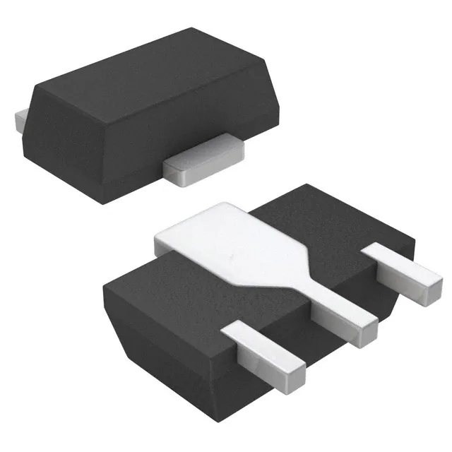
onsemi 2SB1302T-TD-E
- Part No.:
- 2SB1302T-TD-E
- Manufacturer:
- onsemi
- Category:
- Single Bipolar Transistors
- Package:
- TO-243AA
- Datasheet:
-
 2SB1302T-TD-E.pdf
- Description:
- TRANS PNP 20V 5A PCP
- Quantity:
- Payment:

- Shipping:

Inventory:7,065
Please send an inquiry. Send us your inquiry, and we will respond immediately.
Product details
Overview
2SB1302T-TD-E from onsemi is a PNP bipolar junction transistor rated for −20 V VCEO, −5 A IC, and 1.3 W power dissipation in SOT-89 package, featuring low −250 mV typical VCE(sat) at −3 A/−60 mA drive and 320 MHz fT; used in relay drivers and DC-DC converter switching stages.
For engineers reviewing the 2SB1302T-TD-E datasheet, pinout, applications, or equivalent options, key selection criteria include verified −20 V breakdown rating, confirmed SOT-89 thermal performance on ceramic substrate, documented hFE rank T (200–400 at 500 mA), and validated fast switching (ton = 40 ns, tf = 10 ns).
Technical Context
This PNP transistor employs FBET and MBIT fabrication processes to achieve low saturation voltage and high current gain uniformity across its hFE Rank T bin (200–400 at IC = −500 mA). Its −25 V VCBO and −5 V VEBO support robust blocking in negative-rail control circuits.
Designed for high-density hybrid IC integration, it delivers 320 MHz fT with 60 pF Cob at −10 V VCB, enabling reliable operation in medium-frequency switching applications up to several hundred kHz without parasitic oscillation.
Key Specifications
| Parameter | Value and Actual Design Meaning |
|---|---|
| VCEO | −20 V - Maximum safe collector-emitter reverse bias before breakdown in common-emitter configuration. |
| IC | −5 A - Continuous DC collector current rating defining maximum steady-state load drive capability. |
| VCE(sat) | −250 to −500 mV - Confirmed low-saturation voltage at −3 A/−60 mA, reducing conduction loss in switching nodes. |
| hFE Rank | T (200–400) - Guaranteed DC current gain range at −500 mA, enabling predictable base drive sizing. |
| fT | 320 MHz - Gain-bandwidth product confirming usable frequency response for fast-switching control loops. |
| tf | 10 ns - Measured fall time under defined test conditions, supporting ≤10 MHz switching frequencies. |
| PC | 1.3 W - Thermal power limit when mounted on 250 mm² × 0.8 mm ceramic substrate, dictating heatsinking requirements. |
Pinout & Package
SOT-89 (Case 419AU), surface-mount plastic package measuring 4.50 × 2.50 × 1.50 mm with 1.50 mm lead pitch; thermally optimized for ceramic substrate mounting.
| Pin/Terminal | Circuit Role | Design Meaning |
|---|---|---|
| 1 | Base | Control terminal accepting negative base current to enable PNP conduction; requires current-limiting resistor in series. |
| 2 | Collector | Main current-carrying terminal connected to negative supply rail in high-side switch configurations. |
| 3 | Emitter | Output terminal tied to load or ground return path; serves as reference node for base-emitter biasing. |
Key Features
| Feature | Design Value |
|---|---|
| Low VCE(sat) | −250 mV typical at −3 A ensures <0.75 W conduction loss, critical for thermal management in compact DC-DC modules. |
| Fast switching | 40 ns ton, 10 ns tf enables efficient operation at 500 kHz–1 MHz PWM frequencies with minimal dead-time penalty. |
| High hFE consistency | Rank T bin (200–400) reduces base drive variability across production lots, simplifying gate driver design. |
| RoHS-compliant packaging | Pb-free SOT-89 construction meets global environmental regulations without compromising thermal or mechanical reliability. |
Applications
| Relay Drivers | DC-DC Converter Switches |
|---|---|
Use Scenario: Driving electromagnetic relays requiring −5 A peak coil current with fast turn-off to prevent contact arcing. IC Role / Device Role / Timing Role: High-current PNP switch controlling relay coil energization/de-energization in industrial PLC output stages. Use Value: Low −250 mV VCE(sat) minimizes power dissipation during hold state, extending relay lifetime and reducing board heating. | Use Scenario: Serving as synchronous rectifier or main switch in non-isolated buck converters operating at 200–500 kHz. IC Role / Device Role / Timing Role: Power switching element handling −5 A load current with controlled rise/fall edges to reduce EMI. Use Value: 320 MHz fT and 10 ns tf support stable closed-loop regulation without phase margin erosion. |
| Lamp Drivers | Motor Driver Stages |
Use Scenario: Controlling incandescent or halogen lamp loads up to 60 W in automotive interior lighting systems. IC Role / Device Role / Timing Role: High-side current sink switching lamp cathodes to chassis ground in 12 V negative-ground architectures. Use Value: −20 V VCEO withstands load-dump transients up to −18 V, ensuring robustness against automotive electrical noise. | Use Scenario: Implementing H-bridge half-bridge legs for brushed DC motor control in power tools and HVAC actuators. IC Role / Device Role / Timing Role: Complementary PNP device paired with NPN counterparts to deliver bidirectional current flow with matched timing. Use Value: Matched ton/tf characteristics between complementary pairs minimize shoot-through risk during commutation. |
Equivalent & Alternatives
The following parts are listed as comparable options for similar PNP transistor applications.
| Alternative Part | Technical Difference | Application Difference | Selection Advice |
|---|---|---|---|
| 2SB1218T-TD-E | Lower IC (−3 A), higher VCE(sat) (−400 mV typ), same SOT-89 package | Reduced current capacity limits use in >3 A relay or motor loads | Select when lower cost and reduced thermal demand justify 40% lower current rating. |
| MMBT4403LT1G | Smaller SOT-23 package, lower IC (−600 mA), higher VCE(sat) (−750 mV typ) | Not suitable for >1 A loads; limited to signal-level or low-power switching | Choose only for space-constrained PCBs where current demand is below 0.6 A. |
Compared with 2SB1302T-TD-E, 2SB1218T-TD-E offers cost savings at the expense of 40% lower current drive and higher conduction loss, while MMBT4403LT1G sacrifices both current and thermal capability for ultra-compact footprint-neither is pin-compatible, requiring layout revision.
Availability
2SB1302T-TD-E is available at Aetrix Electronics and suitable for relay drivers, DC-DC converter switches, and lamp drivers requiring stable component supply with guaranteed RoHS compliance and traceable lot history.
Supply support for 2SB1302T-TD-E includes scheduled delivery planning, volume procurement assistance, BOM continuity management, traceable sourcing, and lifecycle availability coordination for OEM customers, industrial embedded developers, connected-device designers, and electronics production programs.
Manufacturer
onsemi (formerly ON Semiconductor) is a global semiconductor supplier specializing in energy-efficient power, analog, sensor, and connectivity solutions for automotive, industrial, and cloud infrastructure markets.
The 2SB1302T-TD-E belongs to onsemi's PCP (Power Compact Package) family of PNP transistors engineered for high-current density switching in space-constrained power conversion and electromechanical control applications.
FAQ
What is the maximum continuous collector current rating for the 2SB1302T-TD-E?
The 2SB1302T-TD-E is rated for −5 A continuous collector current (IC) at Ta = 25°C when mounted on a 250 mm² × 0.8 mm ceramic substrate. This rating assumes proper thermal management; derating is required above 25°C ambient per the PC–Ta curve in the datasheet. The 2SB1302T-TD-E must not exceed this limit to ensure long-term reliability and avoid junction overheating.
Does the 2SB1302T-TD-E have a specified gain-bandwidth product?
Yes, the 2SB1302T-TD-E has a guaranteed minimum fT of 320 MHz at VCE = −5 V and IC = −200 mA. This parameter confirms its suitability for medium-frequency switching applications such as DC-DC converters operating up to several hundred kHz. The 2SB1302T-TD-E maintains usable gain well into the MHz range, supporting stable feedback loop design without excessive phase lag.
What is the pin configuration of the 2SB1302T-TD-E in its SOT-89 package?
The 2SB1302T-TD-E uses standard SOT-89 pinout: Pin 1 is Base, Pin 2 is Collector, and Pin 3 is Emitter. This configuration is verified in the official onsemi marking diagram and mechanical outline (Case 419AU). The 2SB1302T-TD-E requires correct orientation during placement to avoid functional failure-Collector (Pin 2) connects to the negative rail, Emitter (Pin 3) to load return.
Is the 2SB1302T-TD-E RoHS compliant and lead-free?
Yes, the 2SB1302T-TD-E is explicitly marked Pb-Free and RoHS compliant per the onsemi datasheet revision dated August 2024. It contains no lead, mercury, cadmium, hexavalent chromium, polybrominated biphenyls (PBB), or polybrominated diphenyl ethers (PBDE). The 2SB1302T-TD-E meets EU Directive 2011/65/EU and subsequent amendments, making it suitable for environmentally regulated end equipment.
How does the hFE Rank T specification affect circuit design for the 2SB1302T-TD-E?
The 2SB1302T-TD-E is binned to Rank T, guaranteeing hFE between 200 and 400 at VCE = −2 V and IC = −500 mA. This tight gain spread allows precise base resistor calculation-e.g., for −3 A load, IB can be sized between −7.5 mA and −15 mA. The 2SB1302T-TD-E's consistent hFE reduces need for overdesign and improves batch-to-batch performance predictability in production.
2SB1302T-TD-E Specifications
- Product attributes
- Attribute value
- Manufacturer:
- onsemi
- Series:
- -
- Package/Case:
- TO-243AA
- Packaging:
- Tape & Reel (TR)
- Product Status:
- Obsolete
- Transistor Type:
- PNP
- Current - Collector (Ic) (Max):
- 5 A
- Voltage - Collector Emitter Breakdown (Max):
- 20 V
- Vce Saturation (Max) @ Ib, Ic:
- 500mV @ 60mA, 3A
- Current - Collector Cutoff (Max):
- 500nA (ICBO)
- DC Current Gain (hFE) (Min) @ Ic, Vce:
- 100 @ 500mA, 2V
- Power - Max:
- 1.3 W
- Frequency - Transition:
- 320MHz
- Operating Temperature:
- 150°C (TJ)
- Grade:
- -
- Qualification:
- -
- Mounting Type:
- Surface Mount
- Supplier Device Package:
- PCP
2SB1302T-TD-E FAQ
1.How can I place an order for 2SB1302T-TD-E through Aetrix?
Please submit a Request for Quotation (RFQ) for 2SB1302T-TD-E on Aetrix. Our sales agent will provide a competitive quotation and guide you through the order confirmation once you accept the terms.
2.Are the price and stock information for 2SB1302T-TD-E reliable?
The price and inventory of 2SB1302T-TD-E are updated periodically and may fluctuate due to market conditions. Stock and pricing data are typically refreshed every 24 hours. Quotation validity for 2SB1302T-TD-E is usually 5 days.
3.What payment methods are accepted for 2SB1302T-TD-E?
We accept Wire Transfer, PayPal, Credit Card, Western Union, MoneyGram, and Escrow for 2SB1302T-TD-E transactions.
Note: Certain payment methods may incur a processing fee.
4.How is shipping managed for 2SB1302T-TD-E?
2SB1302T-TD-E orders can be shipped via leading logistics carriers, including DHL, UPS, FedEx, TNT, or Registered Mail.
Once your 2SB1302T-TD-E order is processed, you will receive an email with the shipment details and tracking number.
Note: Tracking information may take up to 24 hours to appear. Express delivery typically takes 3–5 business days.
5.How can I obtain technical support or documentation for 2SB1302T-TD-E?
For technical support, including 2SB1302T-TD-E datasheets, pinout diagrams, or application guidance, please contact our engineering support team. They can provide detailed documentation and assistance for your 2SB1302T-TD-E requirements.
6.How does Aetrix verify that 2SB1302T-TD-E is sourced from the original manufacturer or authorized distributors?
All 2SB1302T-TD-E products on Aetrix are procured from qualified distributors and authorized channels. Our dedicated quality assurance team conducts strict verification, including traceability checks and, if necessary, third-party testing. This ensures that 2SB1302T-TD-E meets industry standards.
7.What is the process for return or replacement of 2SB1302T-TD-E?
All 2SB1302T-TD-E units undergo pre-shipment inspection (PSI). If there is an issue with 2SB1302T-TD-E, returns or replacements are accepted under the following conditions:
1.Quantity discrepancies, incorrect items, or visible external defects (such as breakage or corrosion), acknowledged by Aetrix.
2.The issue is reported within 90 days of delivery.
3.The 2SB1302T-TD-E part is unused and in its original packaging.
Return procedure for 2SB1302T-TD-E:
1.Submit a request within 90 days.
2.Obtain a Return Material Authorization (RMA) from Aetrix.
2SB1302T-TD-E Tags
-
MMBT3906LT1G
onsemi
-
MMBT3904-7-F
Diodes Incorporated
-
MMBT3904LT1G
onsemi
-
MMBT3906-7-F
Diodes Incorporated
-
MMBT3904-TP
Micro Commercial Co
-
MMBT2222A-7-F
Diodes Incorporated
-
BC846BLT1G
onsemi
-
BC847B,215
Nexperia USA Inc.
-
SMMBT3904LT1G
onsemi
-
MMBT2222A-TP
Micro Commercial Co
-
MMBTA06LT1G
onsemi
-
MMBT2222ALT1G
onsemi
Tech Hub

Counterfeit components can hide behind convincing markings and passing basic function tests. This engineering reference covers source traceability, external inspection, X-ray, XRF, electrical testing, …

A practical engineering and sourcing framework covering lifecycle verification, lifetime-buy calculations, replacement qualification, supplier checks and counterfeit-risk controls.

TTL and CMOS logic families differ in thresholds, loading, output drive, power and timing. This engineering guide compares 74HC and 74HCT, calculates noise margins and checks 3.3 V/5 V compatibility.

A practical engineering guide to 3.3V and 5V logic compatibility, input thresholds, resistor dividers, translator ICs, MOSFET level shifting, I2C pull-ups, timing limits and power-sequencing risks.

The 74HC595 uses push-pull logic outputs, while the TPIC6B595 uses 50 V open-drain DMOS sinks for higher-power loads. This guide compares timing, current limits, 3.3 V interfacing, load wiring, thermal…

The 74HC595 converts serial data into eight stable parallel outputs. This guide covers pin functions, shift and storage timing, OE and MR behavior, drive-current limits, cascading, voltage compatibilit…

A technical comparison of level-sensitive latches and edge-triggered flip-flops, covering timing windows, setup and hold limits, master–slave operation, time borrowing, race-through, HDL inference and…

A D latch stores one bit while Enable controls when data can pass. This reference covers gate-level operation, truth tables, transparency, setup and hold timing, LE versus OE, common ICs and practical …

An SR latch stores one bit through cross-coupled feedback. This engineering reference covers NOR and NAND implementations, truth tables, forbidden-state recovery, gated operation, switch debouncing, fa…

Latch circuits retain one bit through feedback. This technical reference covers SR and D latches, truth tables, transparency, timing limits, latch-versus-flip-flop behavior, applications and common log…


