
 My Inquiry
 My Account


Skyworks Solutions Inc. 515CCA12M8000CAGR
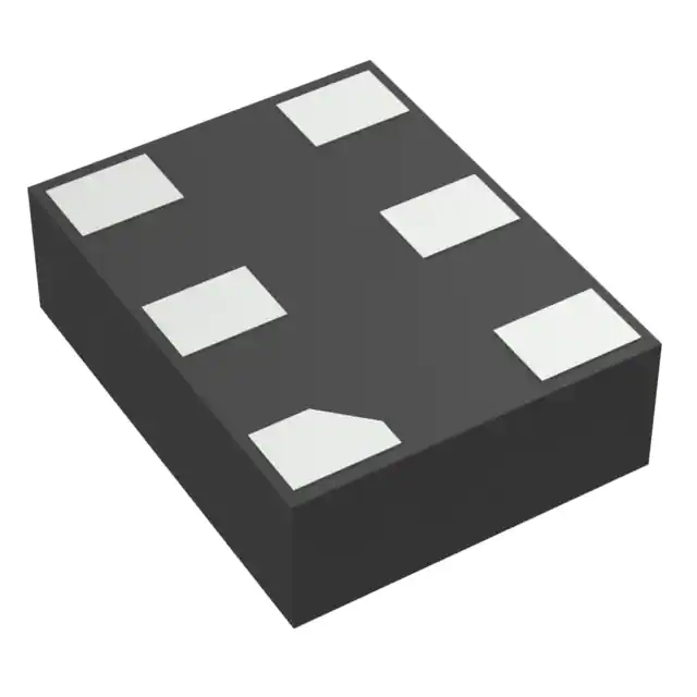
- Part No.:
- 515CCA12M8000CAGR
- Manufacturer:
- Skyworks Solutions Inc.
- Category:
- Oscillators
- Package:
- 6-SMD, No Lead
- Datasheet:
-
 515CCA12M8000CAGR.pdf
- Description:
- DIFFERENTIAL/SINGLE-ENDED SINGLE
- Quantity:
- Payment:

- Shipping:

Inventory:7,825
Please send an inquiry. Send us your inquiry, and we will respond immediately.
Product details
Overview
515CCA12M8000CAGR from Skyworks Solutions is a voltage-controlled crystal oscillator (VCXO) delivering 12.800 MHz output with ±20 ppm temperature stability, ±50 ppm absolute pull range, and 3.3 V CMOS output. It uses an integrated PLL-based synthesizer with a fixed AT-cut fundamental-mode crystal for high reliability and low aging. This device serves as the precision clock source in telecom line cards requiring stable frequency control under varying voltage and thermal conditions.
For engineers reviewing the 515CCA12M8000CAGR datasheet, 515CCA12M8000CAGR pinout, 515CCA12M8000CAGR application, or 515CCA12M8000CAGR equivalent, key selection criteria include its 12.8 MHz nominal frequency, CMOS output drive capability (±8 mA at 3.3 V), 1% control voltage linearity, 10 ms startup time, and 2.5×3.2 mm surface-mount package compatibility with industrial temperature range (–40 to +85 °C).
Technical Context
The 515CCA12M8000CAGR implements Skyworks' proprietary PLL-based frequency synthesis architecture, enabling any frequency from 100 kHz to 212.5 MHz (CMOS variant limit) using a single fixed-frequency crystal resonator. Its control voltage input (Vc) accepts 0.1×VDD to 0.9×VDD with selectable Kv of ±90 ppm/V (per second option code 'C'), and features internal OE polarity configuration with pull-up resistor.
It integrates power supply filtering and ADC-based tuning path for high PSRR (>4 ps additive jitter at 100–500 kHz noise), supports tristate operation with <22 mA disable current, and achieves 0.25–0.35 ps RMS phase jitter (1.875 MHz–20 MHz integration) in CMOS mode - critical for low-jitter PLL reference applications in PON and xDSL systems.
Key Specifications
| Parameter | Value and Actual Design Meaning |
|---|---|
| Nominal Frequency | 12.800 MHz - factory-programmed exact output; enables precise timing alignment in SONET/SDH framers and Ethernet PHYs. |
| Output Format | CMOS - single-ended, rail-to-rail swing (0.15×VDD low / 0.85×VDD high), 0.6–1.2 ns rise/fall time, suitable for FPGA clock inputs and ASIC reset synchronization. |
| Supply Voltage | 3.3 V ±10% - standard logic rail; draws 24–29 mA typical at 100 MHz (scaled lower at 12.8 MHz), compatible with common LDO-regulated power domains. |
| Tuning Slope (Kv) | ±90 ppm/V - linear control sensitivity over 0.33–2.97 V range; enables predictable frequency adjustment in closed-loop clock recovery circuits. |
| Temperature Stability | ±20 ppm over –40 to +85 °C - ensures frequency deviation remains within 256 Hz at 12.8 MHz across full industrial operating range. |
| Aging | ±8.5 ppm over 10 years - guarantees long-term accuracy without field recalibration in deployed telecom infrastructure equipment. |
| Startup Time | ≤10 ms - meets fast-boot requirements in carrier-grade switches and optical line terminals needing rapid clock availability after power-on. |
Pinout & Package
515CCA12M8000CAGR is housed in a RoHS-compliant, lead-free 2.5 × 3.2 mm 6-pin surface-mount package (package code 'C' per ordering guide). The footprint conforms to JEDEC MO-220 and IPC-7351 standards, with 1.25 mm pitch and NSMD land pattern (C1 = 1.9 mm, X1 = 0.70 mm, Y1 = 1.05 mm).
| Pin/Terminal | Circuit Role | Design Meaning |
|---|---|---|
| 1 | Vc | Control voltage input; accepts analog tuning signal (0.33–2.97 V); 100 kΩ input impedance minimizes loading on external DAC or loop filter. |
| 2 | OE | Output enable; active-high with internal 45 kΩ pull-up; asserts tristate when low, reducing system power during idle states. |
| 3 | GND | Electrical and case ground; must be connected to low-impedance PCB ground plane to maintain jitter performance and EMI integrity. |
| 4 | CLK | CMOS clock output; 3.3 V rail-to-rail swing; drives up to 15 pF load with sub-nanosecond edge rates; no termination required. |
| 5 | NC | No connect; left unconnected per datasheet; floating pin must not be tied to VDD, GND, or other signals to avoid parasitic coupling. |
| 6 | VDD | 3.3 V power supply; requires local 100 nF ceramic decoupling adjacent to pin; sensitive to supply ripple due to PLL sensitivity. |
Key Features
| Feature | Design Value |
|---|---|
| Any-frequency synthesis | 12.800 MHz generated via on-chip PLL from fixed crystal - eliminates custom crystal procurement and reduces BOM complexity. |
| High power supply noise rejection | ≤4.0 ps added jitter under 100 mVPP 100–500 kHz supply noise - enables direct use in noisy digital power domains without dedicated LDO. |
| 1% control voltage linearity | BSL error ≤±1% across 10–90% VDD range - ensures monotonic, predictable tuning response in analog control loops. |
| Short lead times | Factory-configured and shipped in <2 weeks - avoids 12–16 week custom oscillator wait times for legacy VCXOs. |
| AT-cut fundamental crystal | Low aging (±8.5 ppm/10 yr) and high mechanical robustness - improves MTBF in vibration-prone telecom chassis and outdoor cabinets. |
Applications
| SONET/SDH Line Cards | PON Optical Line Terminals |
|---|---|
|
Use Scenario: Synchronous optical network transport layer requiring traceable, low-drift reference clocks for STS-192/STM-64 framing and pointer processing. IC Role / Device Role / Timing Role: Primary VCXO reference for clock data recovery (CDR) and elastic store buffers, locked to incoming line rate. Use Value: ±20 ppm stability and ±8.5 ppm aging ensure frame sync loss remains below ITU-T G.823 limits over 10-year deployment life. |
Use Scenario: GPON/EPON OLT systems needing precise 12.8 MHz clock for burst-mode upstream TDMA scheduling and downstream broadcast timing. IC Role / Device Role / Timing Role: Master timing source for burst-mode receiver calibration and dynamic bandwidth allocation logic. Use Value: 10 ms startup time enables fast channel activation after ONT discovery; CMOS drive directly interfaces with FPGA I/O banks. |
| xDSL Central Office Equipment | Broadcast Video Timing Generators |
|
Use Scenario: DSLAM line cards supporting ADSL2+, VDSL2, and G.fast where clock accuracy impacts spectral mask compliance and crosstalk cancellation. IC Role / Device Role / Timing Role: Low-jitter reference for multi-tone DMT symbol generation and adaptive equalization coefficient updates. Use Value: 0.25–0.35 ps RMS phase jitter (1.875 MHz–20 MHz) maintains >70 dB SNR in high-frequency bins above 17 MHz. |
Use Scenario: SDI/HD-SDI video routers and frame synchronizers requiring genlock-capable, drift-tolerant master clock for SMPTE ST 2081-10 compliance. IC Role / Device Role / Timing Role: Adjustable reference oscillator synchronized to external black burst or tri-level sync signal via Vc input. Use Value: ±90 ppm/V tuning slope allows fine-grained drift correction (<1 ppm step) without external DAC, simplifying analog loop design. |
Equivalent & Alternatives
The following parts are listed as comparable options for similar VCXO applications.
| Alternative Part | Technical Difference | Application Difference | Selection Advice |
|---|---|---|---|
| Si514ACA12M8000CGR | Same Si515 family but Si514 variant; lacks integrated PLL - limited to crystal's fundamental frequency only (no any-frequency synthesis). | Only supports fixed 12.8 MHz; cannot be reprogrammed for other frequencies; no Kv or APR flexibility. | Select only if cost-sensitive, fixed-frequency-only requirement exists and future frequency changes are ruled out. |
| DS3205Z-12.8M | Discrete VCXO with separate crystal + varactor; ±25 ppm stability; 3.3 V CMOS; 15 ppm/V tuning slope; 15 ms startup. | Higher aging (±15 ppm/10 yr); no factory programming; requires external loop filter components. | Choose when legacy discrete design reuse is mandatory or when ultra-low-cost, non-programmable solution suffices. |
Compared with Si514ACA12M8000CGR and DS3205Z-12.8M, the 515CCA12M8000CAGR delivers programmable frequency synthesis, superior aging, faster startup, and integrated tuning linearity - making it optimal for next-gen programmable timing in telecom and broadcast platforms.
Availability
515CCA12M8000CAGR is available at Aetrix Electronics and suitable for SONET/SDH line cards, PON optical line terminals, and xDSL central office equipment requiring stable component supply, short lead times, and guaranteed long-term obsolescence management.
Supply support for 515CCA12M8000CAGR includes scheduled delivery planning, volume procurement assistance, BOM continuity management, traceable sourcing, and lifecycle availability coordination for OEM customers, industrial embedded developers, connected-device designers, and electronics production programs.
Manufacturer
Skyworks Solutions is a global leader in semiconductor innovation for wireless, broadband, automotive, and industrial timing applications, with deep expertise in RF, analog, and mixed-signal IC design.
The Si515 VCXO product line was engineered to replace traditional crystal-based oscillators with programmable, low-jitter, factory-configurable timing solutions for telecom infrastructure, networking, and broadcast video systems.
FAQ
What is the nominal output frequency of the 515CCA12M8000CAGR?
The 515CCA12M8000CAGR is factory-programmed to deliver exactly 12.800 MHz. This value is encoded in the "12M800" segment of the part number and verified per Skyworks' Si515 ordering convention. The device maintains this frequency with ±20 ppm stability across –40 to +85 °C and ±8.5 ppm aging over 10 years.
Does the 515CCA12M8000CAGR support LVDS or LVPECL outputs?
No, the 515CCA12M8000CAGR does not support LVDS or LVPECL outputs. Its first option code 'C' specifies CMOS output format and 3.3 V supply. For LVDS or LVPECL variants, different part numbers are used - e.g., 515BBA12M8000CAGR (LVDS) or 515ABA12M8000CAGR (LVPECL).
What is the control voltage tuning range and slope for the 515CCA12M8000CAGR?
The 515CCA12M8000CAGR has a control voltage (Vc) range of 0.33 V to 2.97 V (0.1×VDD to 0.9×VDD) and a tuning slope (Kv) of ±90 ppm/V, as indicated by the second option code 'C'. Its control voltage linearity is specified at ±1% BSL, ensuring predictable frequency adjustment in analog control loops.
Can the 515CCA12M8000CAGR be used in place of a traditional crystal + VCXO IC combination?
Yes - the 515CCA12M8000CAGR integrates both the crystal resonator and PLL-based synthesizer into a single 2.5×3.2 mm package. Unlike discrete solutions, it eliminates external crystal matching, reduces board space, improves reliability via AT-cut fundamental mode, and removes need for external loop filter components.
What package type and mounting configuration does the 515CCA12M8000CAGR use?
The 515CCA12M8000CAGR uses a 2.5 × 3.2 mm, 6-pin surface-mount package (package code 'C') with gull-wing leads. It follows JEDEC MO-220 and IPC-7351 land pattern guidelines (C1 = 1.9 mm, X1 = 0.70 mm, Y1 = 1.05 mm) and is supplied in tape-and-reel format (suffix 'R').
515CCA12M8000CAGR Specifications
- Product attributes
- Attribute value
- Manufacturer:
- Skyworks Solutions Inc.
- Series:
- Si515
- Package/Case:
- 6-SMD, No Lead
- Packaging:
- Tape & Reel (TR)
- Product Status:
- Active
- Base Resonator:
- Crystal
- Type:
- VCXO
- Frequency:
- 12.8 MHz
- Function:
- Enable/Disable
- Output:
- CMOS
- Voltage - Supply:
- 3.3V
- Frequency Stability:
- ±20ppm
- Absolute Pull Range (APR):
- ±50ppm
- Operating Temperature:
- -40°C ~ 85°C
- Spread Spectrum Bandwidth:
- -
- Current - Supply (Max):
- 29mA
- Ratings:
- -
- Mounting Type:
- Surface Mount
- Supplier Device Package:
- -
- Size / Dimension:
- 0.126" L x 0.098" W (3.20mm x 2.50mm)
- Height - Seated (Max):
- 0.043" (1.10mm)
515CCA12M8000CAGR FAQ
1.How can I place an order for 515CCA12M8000CAGR through Aetrix?
Please submit a Request for Quotation (RFQ) for 515CCA12M8000CAGR on Aetrix. Our sales agent will provide a competitive quotation and guide you through the order confirmation once you accept the terms.
2.Are the price and stock information for 515CCA12M8000CAGR reliable?
The price and inventory of 515CCA12M8000CAGR are updated periodically and may fluctuate due to market conditions. Stock and pricing data are typically refreshed every 24 hours. Quotation validity for 515CCA12M8000CAGR is usually 5 days.
3.What payment methods are accepted for 515CCA12M8000CAGR?
We accept Wire Transfer, PayPal, Credit Card, Western Union, MoneyGram, and Escrow for 515CCA12M8000CAGR transactions.
Note: Certain payment methods may incur a processing fee.
4.How is shipping managed for 515CCA12M8000CAGR?
515CCA12M8000CAGR orders can be shipped via leading logistics carriers, including DHL, UPS, FedEx, TNT, or Registered Mail.
Once your 515CCA12M8000CAGR order is processed, you will receive an email with the shipment details and tracking number.
Note: Tracking information may take up to 24 hours to appear. Express delivery typically takes 3–5 business days.
5.How can I obtain technical support or documentation for 515CCA12M8000CAGR?
For technical support, including 515CCA12M8000CAGR datasheets, pinout diagrams, or application guidance, please contact our engineering support team. They can provide detailed documentation and assistance for your 515CCA12M8000CAGR requirements.
6.How does Aetrix verify that 515CCA12M8000CAGR is sourced from the original manufacturer or authorized distributors?
All 515CCA12M8000CAGR products on Aetrix are procured from qualified distributors and authorized channels. Our dedicated quality assurance team conducts strict verification, including traceability checks and, if necessary, third-party testing. This ensures that 515CCA12M8000CAGR meets industry standards.
7.What is the process for return or replacement of 515CCA12M8000CAGR?
All 515CCA12M8000CAGR units undergo pre-shipment inspection (PSI). If there is an issue with 515CCA12M8000CAGR, returns or replacements are accepted under the following conditions:
1.Quantity discrepancies, incorrect items, or visible external defects (such as breakage or corrosion), acknowledged by Aetrix.
2.The issue is reported within 90 days of delivery.
3.The 515CCA12M8000CAGR part is unused and in its original packaging.
Return procedure for 515CCA12M8000CAGR:
1.Submit a request within 90 days.
2.Obtain a Return Material Authorization (RMA) from Aetrix.
515CCA12M8000CAGR Tags
-
ECS-2333-160-BN-TR
ECS Inc.
-
ECS-2333-240-BN-TR
ECS Inc.
-
KC2016Z25.0000C1KX00
KYOCERA AVX
-0.035-Thick.jpg)
-
ECS-2033-250-BN
ECS Inc.
-
O 25,0-JO32-B-1V3-1-T1-LF
Jauch Quartz
-
SIT1533AI-H4-DCC-32.768E
SiTime
-
ECS-2333-500-BN-TR
ECS Inc.
-
COM1305-50.000-EXT-T-TR
Raltron Electronics
-
SG-210STF 24.0000ML0
EPSON
-
ECS-3225MV-320-CN-TR
ECS Inc.
-
ECS-2033-240-BN
ECS Inc.
-
ECS-2333-120-BN-TR
ECS Inc.
Tech Hub

Counterfeit components can hide behind convincing markings and passing basic function tests. This engineering reference covers source traceability, external inspection, X-ray, XRF, electrical testing, …

A practical engineering and sourcing framework covering lifecycle verification, lifetime-buy calculations, replacement qualification, supplier checks and counterfeit-risk controls.

TTL and CMOS logic families differ in thresholds, loading, output drive, power and timing. This engineering guide compares 74HC and 74HCT, calculates noise margins and checks 3.3 V/5 V compatibility.

A practical engineering guide to 3.3V and 5V logic compatibility, input thresholds, resistor dividers, translator ICs, MOSFET level shifting, I2C pull-ups, timing limits and power-sequencing risks.

The 74HC595 uses push-pull logic outputs, while the TPIC6B595 uses 50 V open-drain DMOS sinks for higher-power loads. This guide compares timing, current limits, 3.3 V interfacing, load wiring, thermal…

The 74HC595 converts serial data into eight stable parallel outputs. This guide covers pin functions, shift and storage timing, OE and MR behavior, drive-current limits, cascading, voltage compatibilit…

A technical comparison of level-sensitive latches and edge-triggered flip-flops, covering timing windows, setup and hold limits, master–slave operation, time borrowing, race-through, HDL inference and…

A D latch stores one bit while Enable controls when data can pass. This reference covers gate-level operation, truth tables, transparency, setup and hold timing, LE versus OE, common ICs and practical …

An SR latch stores one bit through cross-coupled feedback. This engineering reference covers NOR and NAND implementations, truth tables, forbidden-state recovery, gated operation, switch debouncing, fa…

Latch circuits retain one bit through feedback. This technical reference covers SR and D latches, truth tables, transparency, timing limits, latch-versus-flip-flop behavior, applications and common log…


