
 My Inquiry
 My Account


Skyworks Solutions Inc. 516EHA000270BAGR
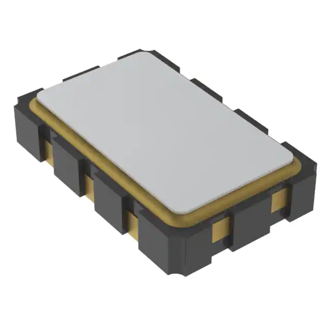
- Part No.:
- 516EHA000270BAGR
- Manufacturer:
- Skyworks Solutions Inc.
- Category:
- Pin Configurable/Selectable Oscillators
- Package:
- 6-SMD, No Lead
- Datasheet:
-
 516EHA000270BAGR.pdf
- Description:
- XTAL OSC VCXO 2.5V 6SMD
- Quantity:
- Payment:

- Shipping:

Inventory:7,411
Please send an inquiry. Send us your inquiry, and we will respond immediately.
Product details
Overview
516EHA000270BAGR from Skyworks Solutions is a dual-frequency voltage-controlled crystal oscillator (VCXO) with factory-programmed output frequencies of 156.25 MHz and 125 MHz, 2.5 V supply, HCSL output format, ±20 ppm temperature stability, ±60 ppm/V tuning slope, and 2.5 × 3.2 mm surface-mount package. It delivers low additive jitter (0.25 ps RMS phase jitter, 1.875–20 MHz) for timing-critical telecom and datacom PLLs.
For engineers reviewing the 516EHA000270BAGR datasheet, 516EHA000270BAGR pinout, 516EHA000270BAGR application, or 516EHA000270BAGR equivalent, this device supports dual-frequency selection via FS pin, offers high power supply noise rejection (3.5 ps jitter increase at 500 kHz), and provides verified HCSL drive capability into 50 Ω loads with 0.73 VPPSE typical swing.
Technical Context
The 516EHA000270BAGR implements an integrated PLL-based synthesizer architecture using a fixed AT-cut fundamental-mode crystal, enabling precise frequency generation across 100 kHz–250 MHz without crystal swaps. Its dual-frequency operation is controlled by a single digital FS input that selects between two factory-configured frequencies.
It features a dedicated analog control voltage (VC) input with ±60 ppm/V Kv, 1% linearity, and 10 kHz modulation bandwidth, supporting fine-tuning in low-jitter clock recovery and synchronization loops. The HCSL output stage drives 50 Ω to ground with 0.38 V common-mode and 0.73 VPPSE swing, meeting JEDEC HCSL-1 standards.
Key Specifications
| Parameter | Value and Actual Design Meaning |
|---|---|
| Nominal Frequencies | 156.25 MHz and 125 MHz - factory-programmed dual outputs for SONET/SDH frame rate switching and FPGA clock domain bridging. |
| Output Format | HCSL - differential output with 0.38 V common-mode and 0.73 VPPSE swing into 50 Ω, compatible with Intel/AMD FPGA clock inputs. |
| Supply Voltage | 2.5 V ±10% - enables direct interface with 2.5 V logic domains and reduces power vs. 3.3 V options (IDD = 44–47 mA typical). |
| Tuning Slope (Kv) | ±60 ppm/V - linear control over ±30 ppm absolute pull range, suitable for narrow-loop PLLs requiring stable VCO gain. |
| Phase Jitter (RMS) | 0.25 ps (1.875–20 MHz) - meets OC-192/STM-64 and 10G Ethernet PHY jitter budgets for clean sampling clocking. |
| Temperature Stability | ±20 ppm (–40 to +85 °C) - ensures frequency accuracy across industrial operating environments without external compensation. |
| Package | 2.5 × 3.2 mm, 6-pin SMD - compact footprint compatible with high-density PCB layouts and automated reflow per JEDEC J-STD-020E. |
Pinout & Package
Package: 2.5 × 3.2 mm, 6-pin surface-mount ceramic package (RoHS-compliant, Pb-free). Pin 1 marked by circle indicator; land pattern per IPC-7351 with NSMD pads and 0.125 mm stencil thickness.
| Pin/Terminal | Circuit Role | Design Meaning |
|---|---|---|
| 1 | Vc | Analog control voltage input (0.1×VDD to 0.9×VDD); sets output frequency within ±30 ppm range with ±60 ppm/V gain. |
| 2 | FS | Digital frequency select input; logic high selects 156.25 MHz, logic low selects 125 MHz (per ordering code B). |
| 3 | GND | Electrical and case ground reference for all internal circuitry and output driver return path. |
| 4 | CLK+ | True-phase HCSL clock output; 0.73 VPPSE swing into 50 Ω, 565 ps rise/fall time, 48–52% duty cycle. |
| 5 | CLK− | Complementary-phase HCSL clock output; maintains 180° phase relationship with CLK+ for differential signaling integrity. |
| 6 | VDD | 2.5 V power supply input; requires local 100 nF ceramic decoupling adjacent to pin for noise suppression. |
Key Features
| Feature | Design Value |
|---|---|
| Dual factory-programmed frequencies | Enables single-device replacement of two discrete VCXOs, reducing BOM count and board space in multi-rate systems. |
| AT-cut fundamental-mode crystal | Delivers <±8.5 ppm aging over 10 years and superior mechanical robustness vs. overtone or MEMS alternatives. |
| High PSRR (3.5 ps jitter @ 500 kHz) | Minimizes need for ultra-clean LDOs; allows shared 2.5 V rail with digital logic while maintaining sub-picosecond jitter. |
| 1% control voltage linearity | Ensures predictable Kv behavior across full VC range, simplifying loop filter design for stable PLL lock. |
| Short lead time (<2 weeks) | Factory programming eliminates NRE and custom crystal procurement delays, accelerating time-to-market for new designs. |
Applications
| SONET/SDH Line Cards | PON OLT Timing |
|---|---|
Use Scenario: Synchronous optical network line cards requiring dual-rate clocking for OC-48 (2.488 Gbps) and OC-192 (9.953 Gbps) framing. IC Role / Device Role / Timing Role: Dual-frequency VCXO providing master reference clocks for SERDES PLLs and framers, selected dynamically via FS pin during protocol handshaking. Use Value: Eliminates need for two separate oscillators and associated layout area; ±20 ppm stability ensures compliance with GR-1244-CORE frequency tolerance requirements. | Use Scenario: Passive optical network optical line terminals synchronizing upstream burst-mode transmissions across multiple wavelengths. IC Role / Device Role / Timing Role: Low-jitter HCSL clock source for TDMA scheduler and burst-mode receiver clock recovery circuits. Use Value: 0.25 ps RMS phase jitter (1.875–20 MHz) meets ITU-T G.984.3 burst-mode jitter mask; 2.5 V operation matches GPON chipset I/O voltage. |
| FPGA-Based Packet Switches | Broadcast Video Sync Generators |
Use Scenario: High-port-count Ethernet switches using FPGAs for packet classification and forwarding, requiring independent 125 MHz and 156.25 MHz clocks for MAC and PHY layers. IC Role / Device Role / Timing Role: Dual-output timing source enabling clock domain crossing between 10GbE PHY and internal fabric logic. Use Value: Single 2.5×3.2 mm package replaces two discrete oscillators; HCSL output directly interfaces with Xilinx UltraScale+ GTY transceivers without level-shifting. | Use Scenario: SMPTE 2110 video-over-IP encoders requiring genlock-capable reference clocks for frame-accurate synchronization across IP streams. IC Role / Device Role / Timing Role: VCXO referenced to external black burst or tri-level sync, tuned via VC input to compensate for network delay variation. Use Value: ±60 ppm/V tuning slope enables precise alignment to SMPTE ST 2059-2 PTP grandmaster clocks; ±20 ppm stability satisfies broadcast-grade timing accuracy. |
Equivalent & Alternatives
The following parts are listed as comparable options for similar dual-frequency VCXO applications.
| Alternative Part | Technical Difference | Application Difference | Selection Advice |
|---|---|---|---|
| Si516EHA000270AAG | Same Si516 family, identical frequencies and tuning slope, but 5×7 mm package instead of 2.5×3.2 mm. | Used where board space permits larger footprint and thermal dissipation is prioritized (θJA = 110°C/W vs. 164°C/W). | Select when PCB layout constraints allow larger package and lower thermal resistance is required for extended ambient temperatures. |
| Si53204-A01870-GM | Multi-output clock generator (not VCXO); no analog VC input; programmable via I²C; higher integration but no voltage tuning. | Replaces VCXO only in systems where digital frequency agility suffices and analog loop control is unnecessary. | Choose when system requires multiple synchronized clocks and digital reconfiguration outweighs need for analog tuning linearity and jitter performance. |
Compared with Si516EHA000270AAG, the 516EHA000270BAGR saves >70% board area and trades 54°C/W higher thermal resistance for compactness; versus Si53204-A01870-GM, it delivers superior analog tuning fidelity and lower jitter but lacks multi-output flexibility.
Availability
516EHA000270BAGR is available at Aetrix Electronics and suitable for SONET/SDH line cards, PON OLT timing modules, and FPGA-based packet switches requiring stable component supply with short lead times and guaranteed long-term continuity.
Supply support for 516EHA000270BAGR includes scheduled delivery planning, volume procurement assistance, BOM continuity management, traceable sourcing, and lifecycle availability coordination for OEM customers, industrial embedded developers, connected-device designers, and electronics production programs.
Manufacturer
Skyworks Solutions is a global semiconductor company specializing in analog and mixed-signal connectivity solutions, with leadership in RF, timing, and precision analog components.
The Si516 product line was designed specifically for high-reliability, low-jitter dual-frequency clock generation in telecom infrastructure, datacenter interconnects, and broadcast equipment where programmable VCXO performance exceeds quartz-only alternatives.
FAQ
What are the exact factory-programmed frequencies of the 516EHA000270BAGR?
The 516EHA000270BAGR is factory-programmed with two precise output frequencies: 156.25 MHz (selected when FS = 1) and 125 MHz (selected when FS = 0), as confirmed by Skyworks' part number lookup utility and ordering documentation for code "000270".
Does the 516EHA000270BAGR support both CMOS and HCSL outputs?
No - the 516EHA000270BAGR is configured exclusively for HCSL output, as indicated by the second option code "H" in its part number. It does not support CMOS; alternative variants like 516EGA000270BAGR (LVDS) or 516ECA000270BAGR (CMOS) would be required for other formats.
What is the absolute pull range specification for the 516EHA000270BAGR?
The 516EHA000270BAGR has a minimum absolute pull range of ±30 ppm, corresponding to its third option code "A" (20 ppm stability, ±60 ppm/V Kv, ±30 ppm APR for 2.5 V operation), per Table on page 14 of the Si516 datasheet Rev. 1.2.
Can the 516EHA000270BAGR operate from a 3.3 V supply?
No - the "E" in the first option code of 516EHA000270BAGR specifies 2.5 V operation. A 3.3 V variant would use option code "A", "B", "C", or "D"; applying 3.3 V to the 516EHA000270BAGR exceeds its absolute maximum VDD rating of +3.8 V only under transient conditions and risks permanent damage.
Is the 516EHA000270BAGR pin-compatible with other Si516 variants in the same package?
Yes - all Si516 devices in the 2.5 × 3.2 mm package share identical 6-pin pinout (Vc, FS, GND, CLK+, CLK−, VDD) and mechanical footprint, enabling drop-in replacement across output format and voltage variants without PCB redesign.
516EHA000270BAGR Specifications
- Product attributes
- Attribute value
- Manufacturer:
- Skyworks Solutions Inc.
- Series:
- Si516
- Package/Case:
- 6-SMD, No Lead
- Packaging:
- Tape & Reel (TR)
- Product Status:
- Active
- Base Resonator:
- Crystal
- Type:
- VCXO
- Frequency - Output 1:
- 148.351648MHz, 148.5MHz
- Frequency - Output 2:
- -
- Frequency - Output 3:
- -
- Frequency - Output 4:
- -
- Function:
- Enable/Disable
- Output:
- LVPECL
- Voltage - Supply:
- 2.5V
- Frequency Stability:
- ±20ppm
- Operating Temperature:
- -40°C ~ 85°C
- Current - Supply (Max):
- 46mA
- Ratings:
- -
- Size / Dimension:
- 0.197" L x 0.126" W (5.00mm x 3.20mm)
- Height:
- 0.052" (1.33mm)
- Supplier Device Package:
- -
516EHA000270BAGR FAQ
1.How can I place an order for 516EHA000270BAGR through Aetrix?
Please submit a Request for Quotation (RFQ) for 516EHA000270BAGR on Aetrix. Our sales agent will provide a competitive quotation and guide you through the order confirmation once you accept the terms.
2.Are the price and stock information for 516EHA000270BAGR reliable?
The price and inventory of 516EHA000270BAGR are updated periodically and may fluctuate due to market conditions. Stock and pricing data are typically refreshed every 24 hours. Quotation validity for 516EHA000270BAGR is usually 5 days.
3.What payment methods are accepted for 516EHA000270BAGR?
We accept Wire Transfer, PayPal, Credit Card, Western Union, MoneyGram, and Escrow for 516EHA000270BAGR transactions.
Note: Certain payment methods may incur a processing fee.
4.How is shipping managed for 516EHA000270BAGR?
516EHA000270BAGR orders can be shipped via leading logistics carriers, including DHL, UPS, FedEx, TNT, or Registered Mail.
Once your 516EHA000270BAGR order is processed, you will receive an email with the shipment details and tracking number.
Note: Tracking information may take up to 24 hours to appear. Express delivery typically takes 3–5 business days.
5.How can I obtain technical support or documentation for 516EHA000270BAGR?
For technical support, including 516EHA000270BAGR datasheets, pinout diagrams, or application guidance, please contact our engineering support team. They can provide detailed documentation and assistance for your 516EHA000270BAGR requirements.
6.How does Aetrix verify that 516EHA000270BAGR is sourced from the original manufacturer or authorized distributors?
All 516EHA000270BAGR products on Aetrix are procured from qualified distributors and authorized channels. Our dedicated quality assurance team conducts strict verification, including traceability checks and, if necessary, third-party testing. This ensures that 516EHA000270BAGR meets industry standards.
7.What is the process for return or replacement of 516EHA000270BAGR?
All 516EHA000270BAGR units undergo pre-shipment inspection (PSI). If there is an issue with 516EHA000270BAGR, returns or replacements are accepted under the following conditions:
1.Quantity discrepancies, incorrect items, or visible external defects (such as breakage or corrosion), acknowledged by Aetrix.
2.The issue is reported within 90 days of delivery.
3.The 516EHA000270BAGR part is unused and in its original packaging.
Return procedure for 516EHA000270BAGR:
1.Submit a request within 90 days.
2.Obtain a Return Material Authorization (RMA) from Aetrix.
516EHA000270BAGR Tags

-
ASEMDHC-L-R
Abracon LLC
-
513FCA000270AAG
Skyworks Solutions Inc.
-
LMK61PD0A2-SIAT
Texas Instruments
-
ASEMDLV-LR
Abracon LLC
2x1,6x0,9.JPG)
-
AMPDAFI-A09T
Abracon LLC
3,2x2,5x0,9.JPG)
-
AMPDEFH-A04T
Abracon LLC
-
534DC000596DG
Skyworks Solutions Inc.
-
ASEMCLV
Abracon LLC
-
DSC6021CI2A-009TT
Microchip Technology
-
DSC6021CI2A-009UT
Microchip Technology
-
DSC6021CI2A-009WT
Microchip Technology
-
DSC6021CI2A-009YT
Microchip Technology
Tech Hub

Counterfeit components can hide behind convincing markings and passing basic function tests. This engineering reference covers source traceability, external inspection, X-ray, XRF, electrical testing, …

A practical engineering and sourcing framework covering lifecycle verification, lifetime-buy calculations, replacement qualification, supplier checks and counterfeit-risk controls.

TTL and CMOS logic families differ in thresholds, loading, output drive, power and timing. This engineering guide compares 74HC and 74HCT, calculates noise margins and checks 3.3 V/5 V compatibility.

A practical engineering guide to 3.3V and 5V logic compatibility, input thresholds, resistor dividers, translator ICs, MOSFET level shifting, I2C pull-ups, timing limits and power-sequencing risks.

The 74HC595 uses push-pull logic outputs, while the TPIC6B595 uses 50 V open-drain DMOS sinks for higher-power loads. This guide compares timing, current limits, 3.3 V interfacing, load wiring, thermal…

The 74HC595 converts serial data into eight stable parallel outputs. This guide covers pin functions, shift and storage timing, OE and MR behavior, drive-current limits, cascading, voltage compatibilit…

A technical comparison of level-sensitive latches and edge-triggered flip-flops, covering timing windows, setup and hold limits, master–slave operation, time borrowing, race-through, HDL inference and…

A D latch stores one bit while Enable controls when data can pass. This reference covers gate-level operation, truth tables, transparency, setup and hold timing, LE versus OE, common ICs and practical …

An SR latch stores one bit through cross-coupled feedback. This engineering reference covers NOR and NAND implementations, truth tables, forbidden-state recovery, gated operation, switch debouncing, fa…

Latch circuits retain one bit through feedback. This technical reference covers SR and D latches, truth tables, transparency, timing limits, latch-versus-flip-flop behavior, applications and common log…


