
 My Inquiry
 My Account


Skyworks Solutions Inc. 544AAJC001967BBG
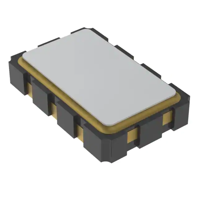
- Part No.:
- 544AAJC001967BBG
- Manufacturer:
- Skyworks Solutions Inc.
- Category:
- Pin Configurable/Selectable Oscillators
- Package:
- 8-SMD, No Lead
- Datasheet:
-
 544AAJC001967BBG.pdf
- Description:
- XTAL OSCILLATOR
- Quantity:
- Payment:

- Shipping:

Inventory:5,002
Please send an inquiry. Send us your inquiry, and we will respond immediately.
Product details
Overview
544AAJC001967BBG from Skyworks Solutions is an I²C-programmable ultra-low-jitter crystal oscillator (XO) delivering user-defined frequencies from 0.2 to 1500 MHz with <1 ppb resolution, 150 fs typical RMS phase jitter (12 kHz–20 MHz), ±7 ppm total frequency stability, and LVDS output in a 3.2 × 5 mm CLCC package - deployed for FPGA/ASIC clocking and 100G optical Ethernet timing.
For engineers reviewing the 544AAJC001967BBG datasheet, 544AAJC001967BBG pinout, 544AAJC001967BBG application, or 544AAJC001967BBG equivalent, this page provides verified electrical specs, factory-configured startup behavior, I²C reprogramming capability, PSNR performance (−83 dBc), and dual CMOS/LVDS format compatibility per Skyworks' Si544 Ultra Series™ datasheet Rev. 206612A.
Technical Context
The 544AAJC001967BBG implements Skyworks' 4th-generation DSPLL® architecture with a fixed 55.05 MHz crystal reference, fractional FBDIV (11.32-bit), integer HSDIV (5–2046), and power-of-2 LSDIV (1–32) to synthesize any frequency across its range while maintaining sub-200 fs jitter. Its digital loop filter and on-chip power supply regulation deliver −83 dBc PSNR at 100–1000 kHz ripple frequencies.
Factory-programmed for LVDS output, 1.8/2.5/3.3 V operation, and ±7 ppm total stability (Grade C), the device supports pin-selectable startup frequencies and I²C Fast Mode Plus (1 Mbps) with guaranteed 100 µs settling for small frequency changes (<±950 ppm) and 40 ms for large transitions including internal VCO calibration.
Key Specifications
| Parameter | Value and Actual Design Meaning |
|---|---|
| Output Frequency Range | 0.2–1500 MHz - supports full-bandwidth synthesis including 156.25 MHz, 200 MHz, and 644.53125 MHz reference clocks |
| Phase Jitter (RMS) | 150 fs typ (12 kHz–20 MHz) - enables compliance with stringent SerDes jitter budgets in 100G/400G coherent optics |
| Total Frequency Stability | ±7 ppm - includes temp, aging (20 yr @ 70°C), initial accuracy, load pulling, and VDD variation |
| Supply Voltage | 1.8 V / 2.5 V / 3.3 V ±5% - single part number supports mixed-voltage system design without BOM variants |
| I²C Interface Speed | Up to 1 Mbps (Fast Mode Plus) - allows rapid field frequency updates without interrupting system operation |
| PSNR Performance | −83 dBc typ @ 100–1000 kHz - rejects noise from switched-mode power supplies without external filtering |
| Package Dimensions | 3.2 × 5 mm CLCC - industry-standard footprint compatible with automated SMT assembly and thermal management (ΘJA = 55 °C/W) |
Pinout & Package
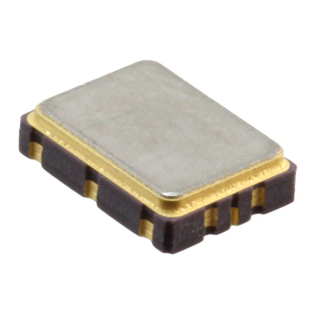
544AAJC001967BBG uses an 8-pin ceramic leadless chip carrier (CLCC) package measuring 3.2 × 5 mm with gull-wing terminations and Au/Ni contact pads (MSL Level 3). Pin functions are validated per Skyworks Si544 datasheet Figure 1 (Top View).
| Pin/Terminal | Circuit Role | Design Meaning |
|---|---|---|
| 1, 2 | Selectable OE/FS/NC | Configurable as output enable (active-high/low), frequency select, or no-connect - polarity and function set at factory |
| 3 | GND | Dedicated ground terminal for low-impedance return path and jitter-sensitive analog core isolation |
| 4 | CLK+ | Differential LVDS clock output positive leg - requires 100 Ω differential termination at receiver |
| 5 | CLK− | Differential LVDS clock output negative leg - complementary to CLK+, unused in CMOS mode |
| 6 | VDD | Single-supply input (1.8/2.5/3.3 V) powering both DSPLL core and LVDS driver - includes on-chip regulation |
| 7 | SDA | I²C bidirectional serial data line - supports 100 kbps/400 kbps/1 Mbps with internal pull-up/pull-down options |
| 8 | SCL | I²C serial clock input - synchronous interface for register writes and frequency reconfiguration |
Key Features
| Feature | Design Value |
|---|---|
| I²C programmability | Any frequency from 0.2–1500 MHz with <1 ppb resolution - eliminates crystal inventory and custom XO lead times |
| Dual CMOS option support | Configurable in-phase or complementary dual outputs - replaces two discrete XOs with one device |
| Multi-voltage operation | 1.8 V / 2.5 V / 3.3 V VDD from same part number - simplifies voltage rail planning in mixed-signal systems |
| Startup frequency flexibility | Up to 4 factory-programmed pin-selectable startup frequencies - ensures deterministic boot-time clocking |
| On-chip PSNR enhancement | −83 dBc typical rejection of 100–1000 kHz supply noise - removes need for dedicated LDO or ferrite beads |
Applications
| 100G/400G Coherent Optics | FPGA/ASIC Clocking |
|---|---|
Use Scenario: Timing reference for DP-QPSK modulators and high-speed ADC/DAC in metro/core DWDM transceivers. IC Role / Device Role / Timing Role: Primary low-jitter clock source synchronizing SERDES lanes and DSP subsystems. Use Value: 150 fs RMS jitter ensures BER <1e−12 under PAM4 modulation; ±7 ppm stability maintains channel alignment over temperature and lifetime. | Use Scenario: Single-clock source for multi-die FPGA clusters with heterogeneous logic, memory, and transceiver banks. IC Role / Device Role / Timing Role: Programmable master oscillator enabling dynamic reconfiguration of logic clock domains via I²C. Use Value: Factory-set startup frequency guarantees deterministic initialization; I²C update allows runtime clock scaling without FPGA recompile. |
| 10G/100G Optical Ethernet | Test & Measurement Equipment |
Use Scenario: Reference clock for IEEE 802.3bs-compliant 100GBASE-LR4 and 400GBASE-DR4 PHYs in switches/routers. IC Role / Device Role / Timing Role: LVDS-output oscillator meeting OIF CEI-28G-LR jitter mask requirements. Use Value: 156.25 MHz and 312.5 MHz synthesis with <200 fs jitter satisfies SONET OC-192 and OTU-4 jitter budgets. | Use Scenario: Precision clock generator in bit-error-rate testers (BERTs), spectrum analyzers, and arbitrary waveform generators. IC Role / Device Role / Timing Role: Ultra-stable, low-phase-noise reference replacing multiple fixed-frequency oscillators. Use Value: −132 dBc/Hz @ 10 kHz offset (200 MHz LVDS) enables accurate spectral purity measurements; I²C tuning supports multi-frequency test sequences. |
Equivalent & Alternatives
The following parts are listed as comparable options for similar programmable oscillator applications.
| Alternative Part | Technical Difference | Application Difference | Selection Advice |
|---|---|---|---|
| Si542ACB001967BBG | Same Si54x family, but Si542 variant with lower max frequency (800 MHz) and ±10 ppm stability (Grade B) | Limited to ≤800 MHz applications; less suitable for 644.53125 MHz PAM4 or 1 GHz+ FPGA clocks | Select only if cost sensitivity outweighs frequency range and stability requirements |
| Si570ACD001967BBG | Legacy DSPLL oscillator with higher jitter (200 fs typ), no factory-programmed startup frequencies, and 2.5×3.2 mm package | Lacks pin-selectable startup modes and has reduced PSNR (−75 dBc); not qualified for extended-temp industrial use | Consider only for legacy redesigns where board space is constrained and jitter margin >50 fs is available |
Compared with Si542ACB001967BBG and Si570ACD001967BBG, the 544AAJC001967BBG delivers broader frequency coverage (0.2–1500 MHz vs. ≤800 MHz), tighter stability (±7 ppm vs. ±10/±20 ppm), and integrated startup configuration - making it optimal for next-gen optical and high-performance computing timing.
Availability
544AAJC001967BBG is available at Aetrix Electronics and suitable for 100G optical Ethernet, FPGA clocking, and test equipment requiring stable component supply, short lead times, and guaranteed long-term availability.
Supply support for 544AAJC001967BBG includes scheduled delivery planning, volume procurement assistance, BOM continuity management, traceable sourcing, and lifecycle availability coordination for OEM customers, industrial embedded developers, connected-device designers, and electronics production programs.
Manufacturer
Skyworks Solutions is a global semiconductor company specializing in analog and mixed-signal connectivity solutions, with leadership in RF, timing, and power management ICs.
The Si544 Ultra Series™ is designed for high-speed digital systems demanding ultra-low jitter, field-programmable frequency agility, and robust supply noise immunity - targeting optical networking, AI accelerators, and advanced test instrumentation.
FAQ
What output frequency range does the 544AAJC001967BBG support?
The 544AAJC001967BBG supports a continuous output frequency range from 0.2 MHz to 1500 MHz with <1 ppb resolution. This includes common standards such as 156.25 MHz (10G Ethernet), 312.5 MHz (25G), and 644.53125 MHz (PAM4), all achievable via I²C programming without hardware changes. The device uses Skyworks' DSPLL® architecture with a fixed 55.05 MHz crystal reference to maintain jitter performance across the full band.
What is the phase jitter specification for the 544AAJC001967BBG?
The 544AAJC001967BBG delivers 150 fs typical RMS phase jitter measured over the 12 kHz to 20 MHz offset band, as specified in Skyworks' Si544 datasheet Rev. 206612A. This value is guaranteed for LVDS, LVPECL, and HCSL outputs and enables compliance with OC-192, OTU-4, and IEEE 802.3bs jitter masks. Measured phase noise reaches −132 dBc/Hz at 10 kHz offset for 200 MHz LVDS output.
Does the 544AAJC001967BBG support multiple supply voltages?
Yes, the 544AAJC001967BBG operates from a single supply voltage of 1.8 V, 2.5 V, or 3.3 V ±5%, with identical performance across all three rails. This multi-voltage capability is built into the same part number and eliminates the need for separate SKUs or voltage-level translation in mixed-voltage systems - confirmed by electrical specifications in Table 2.1 of the official datasheet.
How is the 544AAJC001967BBG configured for startup frequency?
The 544AAJC001967BBG is factory-programmed with up to four user-defined startup frequencies selectable via pins OE/FS0/FS1. For 544AAJC001967BBG specifically, the ordering code "J" indicates quad-frequency select capability with active-high polarity on Pin 2. Startup behavior is non-volatile and persists through power cycles - no I²C initialization is required to begin operation at the designated frequency.
What package type and dimensions does the 544AAJC001967BBG use?
The 544AAJC001967BBG uses a 3.2 × 5 mm ceramic leadless chip carrier (CLCC) package with 8 gull-wing terminals and Au/Ni contact metallization. It complies with MSL Level 3 per JEDEC J-STD-020 and features a thermal resistance of ΘJA = 55 °C/W in still air. This package is optimized for high-frequency signal integrity and thermal dissipation in dense PCB layouts.
544AAJC001967BBG Specifications
- Product attributes
- Attribute value
- Manufacturer:
- Skyworks Solutions Inc.
- Series:
- Ultra™ Si544
- Package/Case:
- 8-SMD, No Lead
- Packaging:
- Strip
- Product Status:
- Not For New Designs
- Base Resonator:
- Crystal
- Type:
- XO (Standard)
- Frequency - Output 1:
- 125MHz, 143.351648MHz, 148.5MHz, 212.5MHz
- Frequency - Output 2:
- -
- Frequency - Output 3:
- -
- Frequency - Output 4:
- -
- Function:
- Enable/Disable
- Output:
- LVPECL
- Voltage - Supply:
- 2.5V, 3.3V
- Frequency Stability:
- ±20ppm
- Operating Temperature:
- -40°C ~ 85°C
- Current - Supply (Max):
- 132mA
- Ratings:
- -
- Size / Dimension:
- 0.197" L x 0.126" W (5.00mm x 3.20mm)
- Height:
- 0.052" (1.33mm)
- Supplier Device Package:
- -
544AAJC001967BBG FAQ
1.How can I place an order for 544AAJC001967BBG through Aetrix?
Please submit a Request for Quotation (RFQ) for 544AAJC001967BBG on Aetrix. Our sales agent will provide a competitive quotation and guide you through the order confirmation once you accept the terms.
2.Are the price and stock information for 544AAJC001967BBG reliable?
The price and inventory of 544AAJC001967BBG are updated periodically and may fluctuate due to market conditions. Stock and pricing data are typically refreshed every 24 hours. Quotation validity for 544AAJC001967BBG is usually 5 days.
3.What payment methods are accepted for 544AAJC001967BBG?
We accept Wire Transfer, PayPal, Credit Card, Western Union, MoneyGram, and Escrow for 544AAJC001967BBG transactions.
Note: Certain payment methods may incur a processing fee.
4.How is shipping managed for 544AAJC001967BBG?
544AAJC001967BBG orders can be shipped via leading logistics carriers, including DHL, UPS, FedEx, TNT, or Registered Mail.
Once your 544AAJC001967BBG order is processed, you will receive an email with the shipment details and tracking number.
Note: Tracking information may take up to 24 hours to appear. Express delivery typically takes 3–5 business days.
5.How can I obtain technical support or documentation for 544AAJC001967BBG?
For technical support, including 544AAJC001967BBG datasheets, pinout diagrams, or application guidance, please contact our engineering support team. They can provide detailed documentation and assistance for your 544AAJC001967BBG requirements.
6.How does Aetrix verify that 544AAJC001967BBG is sourced from the original manufacturer or authorized distributors?
All 544AAJC001967BBG products on Aetrix are procured from qualified distributors and authorized channels. Our dedicated quality assurance team conducts strict verification, including traceability checks and, if necessary, third-party testing. This ensures that 544AAJC001967BBG meets industry standards.
7.What is the process for return or replacement of 544AAJC001967BBG?
All 544AAJC001967BBG units undergo pre-shipment inspection (PSI). If there is an issue with 544AAJC001967BBG, returns or replacements are accepted under the following conditions:
1.Quantity discrepancies, incorrect items, or visible external defects (such as breakage or corrosion), acknowledged by Aetrix.
2.The issue is reported within 90 days of delivery.
3.The 544AAJC001967BBG part is unused and in its original packaging.
Return procedure for 544AAJC001967BBG:
1.Submit a request within 90 days.
2.Obtain a Return Material Authorization (RMA) from Aetrix.
544AAJC001967BBG Tags

-
ASEMDHC-L-R
Abracon LLC
-
513FCA000270AAG
Skyworks Solutions Inc.
-
LMK61PD0A2-SIAT
Texas Instruments
-
ASEMDLV-LR
Abracon LLC
2x1,6x0,9.JPG)
-
AMPDAFI-A09T
Abracon LLC
3,2x2,5x0,9.JPG)
-
AMPDEFH-A04T
Abracon LLC
-
534DC000596DG
Skyworks Solutions Inc.
-
ASEMCLV
Abracon LLC
-
DSC6021CI2A-009TT
Microchip Technology
-
DSC6021CI2A-009UT
Microchip Technology
-
DSC6021CI2A-009WT
Microchip Technology
-
DSC6021CI2A-009YT
Microchip Technology
Tech Hub

Counterfeit components can hide behind convincing markings and passing basic function tests. This engineering reference covers source traceability, external inspection, X-ray, XRF, electrical testing, …

A practical engineering and sourcing framework covering lifecycle verification, lifetime-buy calculations, replacement qualification, supplier checks and counterfeit-risk controls.

TTL and CMOS logic families differ in thresholds, loading, output drive, power and timing. This engineering guide compares 74HC and 74HCT, calculates noise margins and checks 3.3 V/5 V compatibility.

A practical engineering guide to 3.3V and 5V logic compatibility, input thresholds, resistor dividers, translator ICs, MOSFET level shifting, I2C pull-ups, timing limits and power-sequencing risks.

The 74HC595 uses push-pull logic outputs, while the TPIC6B595 uses 50 V open-drain DMOS sinks for higher-power loads. This guide compares timing, current limits, 3.3 V interfacing, load wiring, thermal…

The 74HC595 converts serial data into eight stable parallel outputs. This guide covers pin functions, shift and storage timing, OE and MR behavior, drive-current limits, cascading, voltage compatibilit…

A technical comparison of level-sensitive latches and edge-triggered flip-flops, covering timing windows, setup and hold limits, master–slave operation, time borrowing, race-through, HDL inference and…

A D latch stores one bit while Enable controls when data can pass. This reference covers gate-level operation, truth tables, transparency, setup and hold timing, LE versus OE, common ICs and practical …

An SR latch stores one bit through cross-coupled feedback. This engineering reference covers NOR and NAND implementations, truth tables, forbidden-state recovery, gated operation, switch debouncing, fa…

Latch circuits retain one bit through feedback. This technical reference covers SR and D latches, truth tables, transparency, timing limits, latch-versus-flip-flop behavior, applications and common log…


