
 My Inquiry
 My Account


Texas Instruments 5962-86061012A
- Part No.:
- 5962-86061012A
- Manufacturer:
- Texas Instruments
- Category:
- Signal Switches, Multiplexers, Decoders
- Package:
- -
- Datasheet:
-
 5962-86061012A.pdf
- Description:
- SN54HC157 QUADRUPLE 2-LINE TO 1-
- Quantity:
- Payment:

- Shipping:

Inventory:996
Please send an inquiry. Send us your inquiry, and we will respond immediately.
Product details
Overview
5962-86061012A from Texas Instruments is a military-grade quad 2-line-to-1-line data selector/multiplexer in LCCC-20 ceramic package, operating from −55°C to 125°C with 2 V–6 V supply, 11 ns typical propagation delay at 6 V, ±6-mA output drive, and true-data routing for digital signal selection in hardened systems.
For engineers reviewing the 5962-86061012A datasheet, 5962-86061012A pinout, 5962-86061012A application, or 5962-86061012A equivalent, this device serves as a radiation-tolerant, high-reliability multiplexer for avionics bus arbitration, secure FPGA I/O expansion, and real-time control path selection where extended temperature stability and MIL-PRF-38535 compliance are mandatory.
Technical Context
The 5962-86061012A implements four independent 2:1 multiplexers sharing a common strobe (G) and select (A/B) input, delivering true (non-inverted) outputs. Its CMOS HC logic architecture ensures low static current (≤80 µA) and high noise immunity across full military temperature range.
Each channel routes one of two input pairs (e.g., 1A/1B → 1Y) based on A/B state while G enables/disables all outputs simultaneously. Input transition times are specified down to 400 ns at 6 V, supporting synchronous timing in deterministic embedded control loops.
Key Specifications
| Parameter | Value and Actual Design Meaning |
|---|---|
| Supply Voltage Range | 2 V to 6 V - Enables direct interface with 3.3 V and 5 V logic families without level-shifting. |
| Propagation Delay (tpd) | 11 ns typical at VCC = 6 V, CL = 50 pF - Supports >20 MHz data switching in time-critical routing paths. |
| Output Drive Current | ±6 mA at VCC = 5 V - Sufficient to directly drive 15 LSTTL loads or fan out to multiple downstream gates. |
| Quiescent Current (ICC) | 80 µA max at VCC = 6 V - Enables low-power operation in battery-backed or energy-constrained military subsystems. |
| Operating Temperature | −55°C to +125°C - Qualified per MIL-PRF-38535 Class V for use in aerospace, defense, and downhole instrumentation. |
| Input Leakage Current | 1 µA max - Ensures reliable logic-level recognition even under high-impedance or floating-bus conditions. |
Pinout & Package
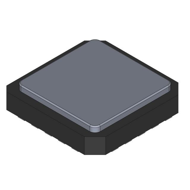
LCCC-20 (FK) ceramic package with 20 leads, hermetically sealed, leadless construction, and no internal connections on pins 3, 9, 10, 11, 12, 17, and 18 (NC). Designed for high-reliability PCB mounting with solder reflow compatibility and minimal thermal stress.
| Pin/Terminal | Circuit Role | Design Meaning |
|---|---|---|
| 1 | A/B Select | Common select line determining source (A or B) for all four channels; active-high logic. |
| 2 | 1A | First channel input A - routed to 1Y when A/B = L and G = L. |
| 3 | NC | No internal connection - must remain unconnected on PCB. |
| 4 | 1B | First channel input B - routed to 1Y when A/B = H and G = L. |
| 5 | 1Y | First channel true output - reflects selected input only when G = L. |
| 6 | 2A | Second channel input A - synchronized with 1A, 3A, 4A via shared A/B and G. |
| 7 | 2B | Second channel input B - paired with 2A for dual-source selection. |
| 8 | 2Y | Second channel true output - disabled (high-impedance) when G = H. |
| 9 | NC | No internal connection - must remain unconnected on PCB. |
| 10 | NC | No internal connection - must remain unconnected on PCB. |
| 11 | NC | No internal connection - must remain unconnected on PCB. |
| 12 | NC | No internal connection - must remain unconnected on PCB. |
| 13 | 3A | Third channel input A - part of 4-channel parallel data path. |
| 14 | 3B | Third channel input B - complements 3A for source selection. |
| 15 | 3Y | Third channel true output - maintains signal integrity with ≤0.33 V VOL at 6 mA sink. |
| 16 | 4A | Fourth channel input A - final channel in quad multiplexer group. |
| 17 | NC | No internal connection - must remain unconnected on PCB. |
| 18 | NC | No internal connection - must remain unconnected on PCB. |
| 19 | 4B | Fourth channel input B - enables dual-source redundancy for critical signals. |
| 20 | VCC | Positive supply terminal - requires local 100-nF ceramic decoupling adjacent to pin. |
Key Features
| Feature | Design Value |
|---|---|
| Quad 2:1 Multiplexer Function | Four independent data paths share one select (A/B) and one enable (G), reducing control wiring and PCB footprint in space-constrained modules. |
| MIL-PRF-38535 Class V Qualification | Meets stringent screening, burn-in, and lot acceptance test requirements for flight-critical electronics in launch vehicles and satellites. |
| True Output Logic | Delivers non-inverted data - eliminates need for external inverters in feedback or monitoring circuits requiring phase coherence. |
| Wide Supply Range (2–6 V) | Supports mixed-voltage system integration without external regulators, simplifying power architecture in hybrid analog-digital boards. |
| Low Input Current (≤1 µA) | Minimizes loading on upstream drivers such as microcontroller GPIOs or precision DAC outputs in sensor interface chains. |
Applications
| Avionics Data Bus Arbitration | FPGA I/O Expansion Interface |
|---|---|
|
Use Scenario: Selecting between primary and backup flight control data streams before feeding into a central processor. IC Role / Device Role / Timing Role: Quad multiplexer providing glitch-free, synchronized switching of four 16-bit telemetry words under hardware-controlled A/B and G signals. Use Value: Eliminates software-based arbitration latency and ensures deterministic <11 ns path delay across all four channels during failover events. |
Use Scenario: Expanding limited FPGA I/O pins to manage multiple sensor banks (e.g., IMU, pressure, temperature) with dynamic reconfiguration. IC Role / Device Role / Timing Role: Hardware-level signal router enabling FPGA to access one of two identical sensor sets per channel without reconfiguring logic fabric. Use Value: Reduces FPGA resource utilization by 4× compared to implementing multiplexing in LUTs, preserving logic for real-time filtering algorithms. |
| Secure Communication Channel Switching | Real-Time Control Path Selection |
|
Use Scenario: Isolating encrypted vs. plaintext communication paths in cryptographic modules based on security mode settings. IC Role / Device Role / Timing Role: Tamper-resistant analog/digital signal selector ensuring physical separation of sensitive data paths with zero cross-talk. Use Value: Meets TEMPEST shielding requirements via LCCC ceramic package and guaranteed high off-isolation (>40 dB) between A/B inputs. |
Use Scenario: Choosing between nominal and safe-mode actuator control signals in autonomous vehicle controllers during fault detection. IC Role / Device Role / Timing Role: Fail-safe multiplexer that defaults to safe-state outputs (G = H forces high-Z) when watchdog timer expires. Use Value: Provides hardware-enforced safety interlock with <100 ns response time, independent of firmware execution state. |
Equivalent & Alternatives
The following parts are listed as comparable options for similar quad 2:1 multiplexer applications.
| Alternative Part | Technical Difference | Application Difference | Selection Advice |
|---|---|---|---|
| SNJ54HC157J | Same logic function and military temp range, but CDIP-16 package with through-hole leads instead of LCCC-20 surface-mount ceramic. | Preferred for legacy board repair or prototyping where manual soldering and socketing are required. | Select SNJ54HC157J only if mechanical compatibility with existing DIP footprints is mandatory and thermal cycling resistance is secondary. |
| SN54HC157W | CFP-16 ceramic flatpack with gull-wing leads; identical electrical specs but different thermal impedance (θJA ≈ 90°C/W vs. LCCC's 75°C/W). | Suitable for conduction-cooled chassis designs where CFP's metal lid provides superior EMI shielding over LCCC. | Choose SN54HC157W when board-level EMI suppression is prioritized over maximum thermal efficiency in sealed enclosures. |
Compared with SNJ54HC157J and SN54HC157W, the 5962-86061012A offers superior thermal performance in surface-mount configurations and tighter mechanical tolerances for automated assembly in high-reliability production lines, making it the preferred choice for new space-qualified designs requiring LCCC packaging.
Availability
5962-86061012A is available at Aetrix Electronics and suitable for avionics data bus arbitration, FPGA I/O expansion, secure communication channel switching, and real-time control path selection requiring stable component supply across extended temperature ranges and long product lifecycles.
Supply support for 5962-86061012A includes scheduled delivery planning, volume procurement assistance, BOM continuity management, traceable sourcing, and lifecycle availability coordination for OEM customers, industrial embedded developers, connected-device designers, and electronics production programs.
Manufacturer
Texas Instruments is a global semiconductor leader specializing in analog, embedded processing, and high-reliability components, with decades of heritage in military and aerospace IC development.
The 5962-86061012A belongs to TI's SN54HC logic family, engineered specifically for mission-critical systems demanding radiation tolerance, extreme temperature resilience, and MIL-PRF-38535 compliance.
FAQ
What is the absolute maximum supply voltage rating for the 5962-86061012A?
The 5962-86061012A has an absolute maximum supply voltage (VCC) rating of −0.5 V to +7 V. Operation beyond 6 V is not recommended for sustained use, as the device is characterized and guaranteed only up to 6 V under recommended operating conditions. Exceeding 7 V risks permanent damage to internal oxide layers.
Does the 5962-86061012A support hot-swap or live-insertion?
No, the 5962-86061012A does not support hot-swap operation. Its absolute maximum ratings do not include power sequencing specifications, and applying VCC before establishing proper GND reference may cause latch-up or excessive current draw. Power must be applied in strict GND-first, VCC-second sequence per MIL-STD-704 guidelines.
How many unused inputs require termination on the 5962-86061012A?
All unused inputs on the 5962-86061012A - including A/B, G, and any unconnected 1A–4B pins - must be terminated to either VCC or GND. Floating CMOS inputs can induce oscillation, increase ICC, and degrade noise margins. TI Application Report SCBA004 mandates this for reliable operation across −55°C to +125°C.
Is the 5962-86061012A pin-compatible with commercial SN74HC157 variants?
No, the 5962-86061012A is not pin-compatible with commercial SN74HC157 variants. It uses a 20-pin LCCC (FK) package with NC pins at positions 3, 9–12, 17, and 18, whereas SN74HC157 packages (D, N, PW, etc.) are 16-pin and assign functional signals to all pins. PCB layout and footprint must be designed specifically for LCCC-20.
What is the meaning of "true data" in the 5962-86061012A description?
"True data" means the 5962-86061012A outputs replicate the selected input signal without inversion - e.g., if 1A = HIGH and A/B = LOW, then 1Y = HIGH. This contrasts with inverting multiplexers (e.g., 'HC158), eliminating the need for external inverters in feedback loops or status monitoring where signal polarity must be preserved.
5962-86061012A Specifications
- Product attributes
- Attribute value
- Manufacturer:
- Texas Instruments
- Series:
- *
- Package/Case:
- -
- Packaging:
- Bulk
- Product Status:
- Active
- Type:
- -
- Circuit:
- -
- Independent Circuits:
- -
- Current - Output High, Low:
- -
- Voltage Supply Source:
- -
- Voltage - Supply:
- -
- Operating Temperature:
- -
- Grade:
- -
- Qualification:
- -
- Mounting Type:
- -
- Supplier Device Package:
- -
5962-86061012A FAQ
1.How can I place an order for 5962-86061012A through Aetrix?
Please submit a Request for Quotation (RFQ) for 5962-86061012A on Aetrix. Our sales agent will provide a competitive quotation and guide you through the order confirmation once you accept the terms.
2.Are the price and stock information for 5962-86061012A reliable?
The price and inventory of 5962-86061012A are updated periodically and may fluctuate due to market conditions. Stock and pricing data are typically refreshed every 24 hours. Quotation validity for 5962-86061012A is usually 5 days.
3.What payment methods are accepted for 5962-86061012A?
We accept Wire Transfer, PayPal, Credit Card, Western Union, MoneyGram, and Escrow for 5962-86061012A transactions.
Note: Certain payment methods may incur a processing fee.
4.How is shipping managed for 5962-86061012A?
5962-86061012A orders can be shipped via leading logistics carriers, including DHL, UPS, FedEx, TNT, or Registered Mail.
Once your 5962-86061012A order is processed, you will receive an email with the shipment details and tracking number.
Note: Tracking information may take up to 24 hours to appear. Express delivery typically takes 3–5 business days.
5.How can I obtain technical support or documentation for 5962-86061012A?
For technical support, including 5962-86061012A datasheets, pinout diagrams, or application guidance, please contact our engineering support team. They can provide detailed documentation and assistance for your 5962-86061012A requirements.
6.How does Aetrix verify that 5962-86061012A is sourced from the original manufacturer or authorized distributors?
All 5962-86061012A products on Aetrix are procured from qualified distributors and authorized channels. Our dedicated quality assurance team conducts strict verification, including traceability checks and, if necessary, third-party testing. This ensures that 5962-86061012A meets industry standards.
7.What is the process for return or replacement of 5962-86061012A?
All 5962-86061012A units undergo pre-shipment inspection (PSI). If there is an issue with 5962-86061012A, returns or replacements are accepted under the following conditions:
1.Quantity discrepancies, incorrect items, or visible external defects (such as breakage or corrosion), acknowledged by Aetrix.
2.The issue is reported within 90 days of delivery.
3.The 5962-86061012A part is unused and in its original packaging.
Return procedure for 5962-86061012A:
1.Submit a request within 90 days.
2.Obtain a Return Material Authorization (RMA) from Aetrix.
5962-86061012A Tags

-
SN74HC138DR
Texas Instruments
-
TC7SB3157CFU,LF(CT
Toshiba Semiconductor and Storage
-
74CBTLV3257PW,118
Nexperia USA Inc.

-
SN74CBTLV3257PWR
Texas Instruments
-
74CBTLV3257GUX
Nexperia USA Inc.
-
74HC154BQ,118
Nexperia USA Inc.

-
P3S0200GMX
NXP USA Inc.

-
SN74CB3Q3245PWR
Texas Instruments
-
SN74CB3Q3257RGYR
Texas Instruments

-
TCA9543APWR
Texas Instruments
-
TCA9546APWR
Texas Instruments

-
SN74HC138N
Texas Instruments
Tech Hub

A practical engineering guide to 3.3V and 5V logic compatibility, input thresholds, resistor dividers, translator ICs, MOSFET level shifting, I2C pull-ups, timing limits and power-sequencing risks.

The 74HC595 uses push-pull logic outputs, while the TPIC6B595 uses 50 V open-drain DMOS sinks for higher-power loads. This guide compares timing, current limits, 3.3 V interfacing, load wiring, thermal…

The 74HC595 converts serial data into eight stable parallel outputs. This guide covers pin functions, shift and storage timing, OE and MR behavior, drive-current limits, cascading, voltage compatibilit…

A technical comparison of level-sensitive latches and edge-triggered flip-flops, covering timing windows, setup and hold limits, master–slave operation, time borrowing, race-through, HDL inference and…

A D latch stores one bit while Enable controls when data can pass. This reference covers gate-level operation, truth tables, transparency, setup and hold timing, LE versus OE, common ICs and practical …

An SR latch stores one bit through cross-coupled feedback. This engineering reference covers NOR and NAND implementations, truth tables, forbidden-state recovery, gated operation, switch debouncing, fa…

Latch circuits retain one bit through feedback. This technical reference covers SR and D latches, truth tables, transparency, timing limits, latch-versus-flip-flop behavior, applications and common log…

An engineering guide to LED driver operation, constant-current and constant-voltage outputs, linear and switching topologies, dimming, IC selection, calculations, replacement compatibility, and fault c…

Operational amplifier guide covering op amp basics, feedback, ideal vs real op amps, common configurations, buffer circuits, offset, bias current, gain-bandwidth, slew rate, rail-to-rail limits and sel…

Jumper cables guide covering safe connection order, red and black clamp placement, final ground connection, cable gauge, length, clamp quality, copper vs CCA cables, jump starter comparison and battery…


