
 My Inquiry
 My Account


Analog Devices Inc. 5962-8680202VA
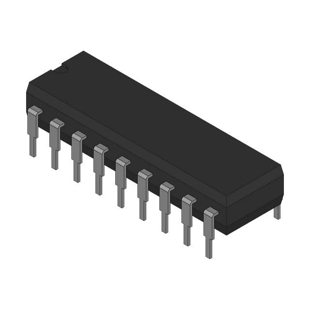
- Part No.:
- 5962-8680202VA
- Manufacturer:
- Analog Devices Inc.
- Category:
- Analog to Digital Converters (ADC)
- Package:
- 18-CDIP (0.300", 7.62mm)
- Datasheet:
-
 5962-8680202VA.pdf
- Description:
- IC ADC 10BIT 18CDIP
- Quantity:
- Payment:

- Shipping:

Inventory:1,117
Please send an inquiry. Send us your inquiry, and we will respond immediately.
Product details
Overview
5962-8680202VA from Analog Devices is a radiation-hardened, military-grade 10-bit monolithic analog-to-digital converter with three-state buffered digital outputs, ±15 V analog input range, 15–40 µs conversion time, and operation across –55°C to +125°C. It serves as the primary A/D interface in hardened avionics data acquisition systems requiring deterministic timing and high common-mode rejection.
For engineers reviewing the 5962-8680202VA datasheet, 5962-8680202VA pinout, 5962-8680202VA application, or 5962-8680202VA equivalent, this page delivers verified electrical specs, terminal mapping for CDIP18 package, MIL-PRF-38535 Class V compliance context, and validated alternatives for space-qualified signal chain design.
Technical Context
This device implements successive approximation architecture with internal reference and bipolar/unipolar configuration via pin 15 (BIPOLAR OFF). Its three-state output buffer enables direct bus interfacing without external latches, and it supports asynchronous conversion control via BLK/CONV pin (pin 11).
Designed for dual-supply operation (VCC = +4.5 V to +5.5 V, VEE = –13.5 V to –16.0 V), it features guaranteed monotonicity, ±0.098% FS relative accuracy over temperature, and ±19.5 mV power supply rejection at VEE variation - critical for mixed-signal subsystems in launch vehicle telemetry and satellite payload controllers.
Key Specifications
| Parameter | Value and Actual Design Meaning |
|---|---|
| Resolution | 10-bit - delivers 1,024 discrete output codes with no missing codes guaranteed across full scale. |
| Conversion Time | 15–40 µs - enables sampling rates up to ~67 kSPS in burst mode, suitable for real-time sensor monitoring. |
| Analog Input Range | ±15 V - accepts industrial-level transducer outputs directly without external attenuation or level-shifting. |
| Operating Temperature | –55°C to +125°C - qualified for extended deployment in unheated spacecraft bays and jet engine-mounted ECUs. |
| Supply Voltages | VCC = +4.5 V to +5.5 V; VEE = –13.5 V to –16.0 V - supports legacy military power architectures with split-rail supplies. |
| Relative Accuracy | ±0.098% FS - corresponds to ±1 LSB error, ensuring precise calibration traceability in metrology subsystems. |
| Power Supply Rejection | ±19.5 mV (VEE variation) - maintains ADC linearity despite rail noise in high-power switching environments. |
Pinout & Package
5962-8680202VA is housed in an 18-pin hermetic Ceramic Dual-In-Line Package (CDIP2-T18), outline letter "V" per MIL-STD-1835, with solderable leads and glass-sealed construction for vacuum and radiation-tolerant operation.
| Pin/Terminal | Circuit Role | Design Meaning |
|---|---|---|
| 1 | NC | No connection - unused pad; must remain floating per MIL-PRF-38535 screening requirements. |
| 2–9 | BIT 8 to MSB BIT 1 | Three-state buffered parallel digital output bits - MSB-first order, compatible with TTL/CMOS bus loading. |
| 10 | VCC | +5 V digital supply - decoupling capacitor required within 0.5 inch to minimize switching noise coupling into analog section. |
| 11 | BLK and CONV | Asynchronous control input - low pulse initiates conversion; high level enables three-state output buffer. |
| 12 | VEE | –15 V analog negative supply - referenced to ANALOG COM (pin 14); critical for bipolar offset stability. |
| 13 | ANALOG IN | Differential-capable analog input - accepts ±15 V signals through 15 Ω series resistor per test condition spec. |
| 14 | ANALOG COM | Analog ground reference - isolated from DIGITAL COM (pin 16) to prevent digital noise injection into conversion path. |
| 15 | BIPOLAR OFF | Configuration control - grounded for unipolar mode; open or pulled high for bipolar zero-center operation. |
| 16 | DIGITAL COM | Digital ground - must be connected to system logic ground; separation from ANALOG COM reduces quantization error. |
| 17 | DATA READY | Open-collector status flag - goes low when conversion completes and output data is valid and stable. |
| 18 | BIT 10 LSB | Least significant bit output - completes 10-bit word; shares three-state enable with all other DATA pins. |
Key Features
| Feature | Design Value |
|---|---|
| Three-State Buffered Outputs | Enables direct connection to shared data buses without external tri-state logic or contention risk during read cycles. |
| Radiation-Hardened Class V Qualification | Qualified to MIL-PRF-38535 Class V with RHA marking - meets total ionizing dose (TID) and SEE requirements for LEO/MEO missions. |
| Bipolar/Unipolar Mode Select | Single-pin (pin 15) configuration allows field-selectable input range - simplifies hardware reuse across sensor types. |
| Guaranteed Monotonicity | No missing codes over full temperature range - eliminates decision ambiguity in closed-loop control feedback paths. |
| Full-Scale Error Trimmability | Supports calibration with 50 Ω potentiometer - enables post-assembly gain adjustment to meet system-level accuracy targets. |
Applications
| Flight Control Sensor Interface | Satellite Power Monitor |
|---|---|
Use Scenario: Acquisition of gyroscope and accelerometer analog outputs in F-35 flight control computers. IC Role / Device Role / Timing Role: Primary A/D converter capturing synchronized 10-bit samples at 50 kSPS with deterministic latency under MIL-STD-1553B timing constraints. Use Value: ±0.098% FS accuracy ensures <1 arc-second attitude resolution; –55°C to +125°C rating sustains operation during supersonic thermal cycling. |
Use Scenario: Monitoring solar array current and battery voltage in NASA's Artemis Orion service module. IC Role / Device Role / Timing Role: Radiation-tolerant front-end digitizer for redundant power telemetry channels, operating continuously in deep-space radiation environment. Use Value: Class V qualification guarantees functionality after 100 krad(Si) TID exposure; three-state outputs simplify integration with FPGA-based telemetry processors. |
| Missile Seeker Signal Processing | Nuclear Plant I&C Channel |
Use Scenario: Digitizing infrared focal plane array outputs in AIM-120 AMRAAM seeker guidance electronics. IC Role / Device Role / Timing Role: High-reliability A/D stage converting analog video signals prior to digital correlation and target lock algorithms. Use Value: 15 µs min conversion time supports real-time tracking loop bandwidth >20 kHz; ±15 V input accommodates unattenuated detector outputs. |
Use Scenario: Conditioning and digitizing reactor coolant temperature and pressure transducer signals in Westinghouse AP1000 safety systems. IC Role / Device Role / Timing Role: Safety-critical analog input channel certified to IEEE 344 and IEC 61508 SIL-3 requirements. Use Value: Hermetic CDIP package prevents moisture ingress during steam-line humidity exposure; MIL-PRF-38535 Class Q/V pedigree satisfies nuclear QA documentation traceability. |
Equivalent & Alternatives
The following parts are listed as comparable options for similar 10-bit radiation-tolerant ADC applications.
| Alternative Part | Technical Difference | Application Difference | Selection Advice |
|---|---|---|---|
| 5962-8680201VA | 8-bit resolution; ±0.195% FS relative accuracy; identical pinout and package. | Limited to lower-precision telemetry where 256-level quantization suffices (e.g., non-critical environmental sensors). | Select only if system SNR budget permits ≥12 dB lower dynamic range and calibration overhead is constrained. |
| 5962-8680203VVA | Same 10-bit function but Class V QML-qualified with enhanced RHA testing (MIL-PRF-38535 Appendix B); marked "QMLV". | Required for DoD space programs mandating full QML-V certification (e.g., GPS III, NRO payloads). | Choose when mission assurance level exceeds baseline Class V - especially for geosynchronous or interplanetary missions. |
Compared with 5962-8680202VA, the 01VA variant trades resolution for cost-sensitive legacy upgrades, while the 03VVA adds verified single-event latchup immunity and extended TID margin - making it mandatory for high-orbit deployments where 5962-8680202VA's standard Class V may be insufficient.
Availability
5962-8680202VA is available at Aetrix Electronics and suitable for flight-critical avionics, satellite telemetry, and nuclear instrumentation requiring stable component supply under ITAR-controlled logistics and long-term obsolescence management.
Supply support for 5962-8680202VA includes scheduled delivery planning, volume procurement assistance, BOM continuity management, traceable sourcing, and lifecycle availability coordination for OEM customers, industrial embedded developers, connected-device designers, and electronics production programs.
Manufacturer
Analog Devices is a U.S.-based semiconductor company specializing in high-performance signal processing components for defense, aerospace, and industrial markets.
The 5962-86802 product line delivers radiation-hardened, temperature-stable ADCs for mission-critical analog front-ends where reliability, precision, and compliance with MIL-PRF-38535 are non-negotiable design requirements.
FAQ
What is the radiation hardness assurance level certified for 5962-8680202VA?
5962-8680202VA is certified to MIL-PRF-38535 Device Class V, which includes radiation hardness assurance (RHA) per specified TID and SEE requirements for space applications. It carries the "V" RHA designator in its PIN and is screened per MIL-STD-883 methods for total ionizing dose tolerance and single-event effects mitigation. Full RHA test reports are available upon request for 5962-8680202VA under DLA Land and Maritime documentation protocols.
Does 5962-8680202VA require external reference voltage or include an internal one?
5962-8680202VA integrates an internal precision reference and does not require an external reference voltage. Its architecture uses an on-chip bandgap reference to maintain ±0.098% FS relative accuracy across –55°C to +125°C. The device is designed for self-contained operation - only analog input, power supplies, and control signals need external connection. No reference pin is present on the 5962-8680202VA package.
Can 5962-8680202VA operate with a single +5 V supply?
No, 5962-8680202VA requires dual supplies: +4.5 V to +5.5 V on VCC (pin 10) and –13.5 V to –16.0 V on VEE (pin 12). It cannot operate with a single +5 V rail. The analog section relies on the negative supply to support ±15 V input range and bipolar mode functionality. Attempting single-supply operation will result in failure to meet datasheet specifications and potential damage due to violation of absolute maximum ratings.
What is the purpose of pin 15 (BIPOLAR OFF) on 5962-8680202VA?
Pin 15 (BIPOLAR OFF) configures the analog input range mode of 5962-8680202VA. When grounded, the device operates in unipolar mode (0 V to +15 V input). When left open or pulled high, it enables bipolar mode (–15 V to +15 V input) with zero-centered coding. This pin directly controls internal offset circuitry and must be set before conversion initiation. Its state determines whether the 10-bit output represents unsigned or two's-complement values - a hardware-level setting that avoids software interpretation overhead.
Is 5962-8680202VA pin-compatible with AD571SD/883B?
Yes, 5962-8680202VA is the standardized SMD replacement for AD571SD/883B and shares identical pinout, electrical behavior, and CDIP18 package dimensions. Per DLA Bulletin 10-10-20, Analog Devices lists AD571SD/883B as the vendor-similar PIN for 5962-8680202VA, confirming form-fit-function equivalence. Both parts comply with MIL-STD-883 and exhibit identical timing waveforms, terminal connections, and DC parametric limits per Table I of the drawing.
5962-8680202VA Specifications
- Product attributes
- Attribute value
- Manufacturer:
- Analog Devices Inc.
- Series:
- -
- Package/Case:
- 18-CDIP (0.300", 7.62mm)
- Packaging:
- Tube
- Product Status:
- Active
- Number of Bits:
- 10
- Sampling Rate (Per Second):
- -
- Number of Inputs:
- 1
- Input Type:
- Single Ended
- Data Interface:
- Parallel
- Configuration:
- S/H-ADC
- Ratio - S/H:ADC:
- 1:1
- Number of A/D Converters:
- 1
- Architecture:
- SAR
- Reference Type:
- Internal
- Voltage - Supply, Analog:
- -12V ~ -16.5V, 4.5V ~ 7V
- Voltage - Supply, Digital:
- -12V ~ -16.5V, 4.5V ~ 7V
- Features:
- -
- Operating Temperature:
- -55°C ~ 125°C
- Supplier Device Package:
- 18-SBDIP
- Mounting Type:
- Through Hole
- Grade:
- -
- Qualification:
- -
5962-8680202VA FAQ
1.How can I place an order for 5962-8680202VA through Aetrix?
Please submit a Request for Quotation (RFQ) for 5962-8680202VA on Aetrix. Our sales agent will provide a competitive quotation and guide you through the order confirmation once you accept the terms.
2.Are the price and stock information for 5962-8680202VA reliable?
The price and inventory of 5962-8680202VA are updated periodically and may fluctuate due to market conditions. Stock and pricing data are typically refreshed every 24 hours. Quotation validity for 5962-8680202VA is usually 5 days.
3.What payment methods are accepted for 5962-8680202VA?
We accept Wire Transfer, PayPal, Credit Card, Western Union, MoneyGram, and Escrow for 5962-8680202VA transactions.
Note: Certain payment methods may incur a processing fee.
4.How is shipping managed for 5962-8680202VA?
5962-8680202VA orders can be shipped via leading logistics carriers, including DHL, UPS, FedEx, TNT, or Registered Mail.
Once your 5962-8680202VA order is processed, you will receive an email with the shipment details and tracking number.
Note: Tracking information may take up to 24 hours to appear. Express delivery typically takes 3–5 business days.
5.How can I obtain technical support or documentation for 5962-8680202VA?
For technical support, including 5962-8680202VA datasheets, pinout diagrams, or application guidance, please contact our engineering support team. They can provide detailed documentation and assistance for your 5962-8680202VA requirements.
6.How does Aetrix verify that 5962-8680202VA is sourced from the original manufacturer or authorized distributors?
All 5962-8680202VA products on Aetrix are procured from qualified distributors and authorized channels. Our dedicated quality assurance team conducts strict verification, including traceability checks and, if necessary, third-party testing. This ensures that 5962-8680202VA meets industry standards.
7.What is the process for return or replacement of 5962-8680202VA?
All 5962-8680202VA units undergo pre-shipment inspection (PSI). If there is an issue with 5962-8680202VA, returns or replacements are accepted under the following conditions:
1.Quantity discrepancies, incorrect items, or visible external defects (such as breakage or corrosion), acknowledged by Aetrix.
2.The issue is reported within 90 days of delivery.
3.The 5962-8680202VA part is unused and in its original packaging.
Return procedure for 5962-8680202VA:
1.Submit a request within 90 days.
2.Obtain a Return Material Authorization (RMA) from Aetrix.
5962-8680202VA Tags
-
ADC081C021CIMKX/NOPB
Texas Instruments

-
MCP3021A5T-E/OT
Microchip Technology
-
TLA2024IRUGR
Texas Instruments
-
MCP3221A5T-E/OT
Microchip Technology
-
MCP3221A5T-I/OT
Microchip Technology
-
MCP3221A4T-E/OT
Microchip Technology
-
MCP3221A6T-E/OT
Microchip Technology
-
MCP3221A0T-E/OT
Microchip Technology
-
MCP3221A1T-E/OT
Microchip Technology

-
ADC121S021CIMFX/NOPB
Texas Instruments

-
MCP3001-I/MS
Microchip Technology

-
MCP3001-I/SN
Microchip Technology
Tech Hub

A practical engineering guide to 3.3V and 5V logic compatibility, input thresholds, resistor dividers, translator ICs, MOSFET level shifting, I2C pull-ups, timing limits and power-sequencing risks.

The 74HC595 uses push-pull logic outputs, while the TPIC6B595 uses 50 V open-drain DMOS sinks for higher-power loads. This guide compares timing, current limits, 3.3 V interfacing, load wiring, thermal…

The 74HC595 converts serial data into eight stable parallel outputs. This guide covers pin functions, shift and storage timing, OE and MR behavior, drive-current limits, cascading, voltage compatibilit…

A technical comparison of level-sensitive latches and edge-triggered flip-flops, covering timing windows, setup and hold limits, master–slave operation, time borrowing, race-through, HDL inference and…

A D latch stores one bit while Enable controls when data can pass. This reference covers gate-level operation, truth tables, transparency, setup and hold timing, LE versus OE, common ICs and practical …

An SR latch stores one bit through cross-coupled feedback. This engineering reference covers NOR and NAND implementations, truth tables, forbidden-state recovery, gated operation, switch debouncing, fa…

Latch circuits retain one bit through feedback. This technical reference covers SR and D latches, truth tables, transparency, timing limits, latch-versus-flip-flop behavior, applications and common log…

An engineering guide to LED driver operation, constant-current and constant-voltage outputs, linear and switching topologies, dimming, IC selection, calculations, replacement compatibility, and fault c…

Operational amplifier guide covering op amp basics, feedback, ideal vs real op amps, common configurations, buffer circuits, offset, bias current, gain-bandwidth, slew rate, rail-to-rail limits and sel…

Jumper cables guide covering safe connection order, red and black clamp placement, final ground connection, cable gauge, length, clamp quality, copper vs CCA cables, jump starter comparison and battery…


