
 My Inquiry
 My Account


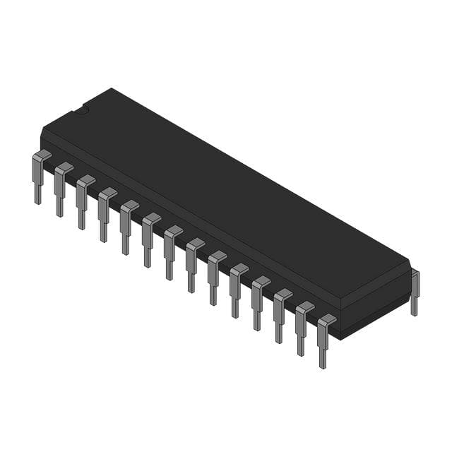
Texas Instruments 5962-9461601QXA
- Part No.:
- 5962-9461601QXA
- Manufacturer:
- Texas Instruments
- Package:
- -
- Datasheet:
-
 5962-9461601QXA.pdf
- Description:
- SN54ABT8652 SCAN TEST DEVICES WI
- Quantity:
- Payment:

- Shipping:

Inventory:1,182
Please send an inquiry. Send us your inquiry, and we will respond immediately.
Product details
Overview
5962-9461601QXA from Texas Instruments is a military-grade scan-test octal bus transceiver with integrated IEEE 1149.1 boundary-scan architecture, dual-directional registered/transparency data flow control (A↔B), and EPIC-IIB BiCMOS process. It operates from –55°C to 125°C, supports JTAG TAP interface (TCK/TMS/TDI/TDO), and delivers 8-bit bidirectional data transfer with clocked register storage and output-enable control. Used in high-reliability avionics and defense system board-level test infrastructure.
For engineers reviewing the 5962-9461601QXA datasheet, 5962-9461601QXA pinout, 5962-9461601QXA application, or 5962-9461601QXA equivalent, this page provides verified functional identity, military temperature validation, IEEE 1149.1 compliance details, boundary-scan register mapping (38-bit BSR), and direct comparison against SN74ABT8652 and SNJ54ABT8652 for legacy design continuity and supply chain migration.
Technical Context
The 5962-9461601QXA implements a dual-mode architecture: normal-function mode replicates 'F652/'ABT652 octal transceiver behavior with CLKAB/CLKBA, SAB/SBA, and OEAB/OEBA controls; test mode disables functional logic and activates IEEE 1149.1 boundary-scan via dedicated TAP controller driving three test registers - 38-bit boundary-scan register (BSR), 11-bit boundary-control register (BCR), and 1-bit bypass register.
Its TAP controller fully complies with IEEE Std 1149.1-1990 state transitions (Test-Logic-Reset → Run-Test/Idle → Shift-DR/IR), captures data on TCK rising edge and updates outputs on falling edge, and supports SCOPE™ instructions including EXTEST, INTEST, SAMPLE/PRELOAD, HIGHZ, CLAMP, RUNT, and BCR-scanning - all validated for MIL-PRF-38535 Class Q/V screening.
Key Specifications
| Parameter | Value and Actual Design Meaning |
|---|---|
| Temperature Range | –55°C to +125°C - Fully characterized and tested per MIL-PRF-38535 for space and defense applications. |
| Boundary-Scan Register | 38-bit BSR - Contains two cells per I/O (input + output) for A1–A8 and B1–B8, plus control pins (OEAB, OEBA, CLKAB, CLKBA, SAB, SBA). |
| TAP Interface | IEEE 1149.1-1990 compliant - Dedicated TCK, TMS, TDI, TDO pins with internal pullups on TMS/TDI; synchronous capture on TCK↑, update on TCK↓. |
| Data Path Control | Dual independent clocking - CLKAB/SAB/OEAB govern A→B flow; CLKBA/SBA/OEBA govern B→A flow, supporting transparent or registered transfer per direction. |
| Process Technology | EPIC-IIB BiCMOS - Delivers TTL-compatible drive strength with reduced power vs. pure bipolar, enabling high-speed (tpd ≤ 5.5 ns typical) operation at military temp extremes. |
| Supply Voltage | VCC = 4.5 V to 5.5 V - Validated across full military range; no derating required at temperature extremes. |
| Package | Ceramic DIP (JT) - Hermetically sealed 28-pin dual in-line package meeting MIL-STD-883 requirements for moisture resistance and thermal cycling. |
Pinout & Package
Ceramic Dual In-Line Package (JT), 28-pin, hermetic, lead finish SnPb per MIL-STD-1835. Pin 1 index corner marked; pin 14 = GND, pin 28 = VCC.
| Pin/Terminal | Circuit Role | Design Meaning |
|---|---|---|
| A1–A8 | Normal-function A-bus I/O | Octal bidirectional data terminals for A-side bus; each has separate input and output boundary-scan cells in BSR. |
| B1–B8 | Normal-function B-bus I/O | Octal bidirectional data terminals for B-side bus; each mapped to two BSR bits (input + output) for full observability/control. |
| CLKAB | A→B clock input | Low-to-high transition clocks A-bus data into A-register; enables real-time or stored A→B transfer depending on SAB state. |
| CLKBA | B→A clock input | Low-to-high transition clocks B-bus data into B-register; enables real-time or stored B→A transfer depending on SBA state. |
| SAB | A→B select input | Low = transparent A→B path; High = registered A→B path using stored A-data; controls functional mode, not scan. |
| SBA | B→A select input | Low = transparent B→A path; High = registered B→A path using stored B-data; independent of SAB timing. |
| OEAB | A→B output enable | Active-high; enables B-output drivers when High; places B1–B8 in high-Z when Low - mapped to BSR bit 37. |
| OEBA | B→A output enable | Active-low; enables A-output drivers when Low; places A1–A8 in high-Z when High - mapped to BSR bit 36. |
| TCK | Test clock | System clock for all boundary-scan operations; data captured on rising edge, outputs updated on falling edge. |
| TMS | Test mode select | Directs TAP controller state transitions; internal pullup ensures Test-Logic-Reset on open/unconnected condition. |
| TDI | Test data input | Serial input for instruction/data register loading; internal pullup holds high if unconnected. |
| TDO | Test data output | Serial output for instruction/data register readback; tri-stated during Shift-DR/Shift-IR until first TCK↓. |
| GND | Ground reference | Pin 14 - primary signal and power return; required for stable boundary-scan cell operation and noise immunity. |
| VCC | Power supply | Pin 28 - 4.5 V to 5.5 V supply; powers both functional logic and boundary-scan circuitry; decoupling mandatory. |
Key Features
| Feature | Design Value |
|---|---|
| IEEE 1149.1 Boundary-Scan Compliance | Fully implemented TAP controller, 38-bit BSR, 11-bit BCR, and BYPASS register - enables automated PCB interconnect test without physical probe access. |
| Dual-Mode Operation | Functional mode operates identically to 'F652/'ABT652; test mode disables functional logic without affecting system timing - zero impact on host design during scan activation. |
| Parallel-Signature Analysis (PSA) | Configurable 16-bit PSA with input masking (BCR bits 10–3) - compresses bus-wide response data into compact signature for fault detection in production test. |
| Pseudo-Random Pattern Generation (PRPG) | On-chip 16-bit PRPG engine driven by BCR - generates stimulus patterns for structural testing of attached logic without external pattern memory. |
| MIL-PRF-38535 Qualification | Class Q or V screening performed - includes burn-in, temperature cycling, hermeticity, and parametric testing across full –55°C to +125°C range. |
| Two BSCs Per I/O | Independent input and output boundary-scan cells for all 16 data lines - enables full visibility of both signal launch and capture points for traceable fault isolation. |
Applications
| Avionics Backplane Diagnostics | Missile Guidance System Test |
|---|---|
|
Use Scenario: Real-time boundary-scan testing of ARINC 429 or MIL-STD-1553 bus interfaces during flight-line maintenance. IC Role / Device Role / Timing Role: Acts as IEEE 1149.1-compliant scan node on critical data buses; provides deterministic TCK-synchronized sampling of A/B bus states during powered self-test. Use Value: Eliminates need for intrusive bed-of-nails fixtures; enables in-system verification of solder joints, connector mating, and routing integrity under operational voltage/temperature. |
Use Scenario: Automated test of guidance computer backplane interconnects during final assembly and depot-level repair. IC Role / Device Role / Timing Role: Functions as boundary-scan controller for multi-board assemblies; executes EXTEST and RUNT (PSA/PRPG) sequences via JTAG daisy-chain. Use Value: Reduces test cycle time by >65% vs. flying-probe methods; detects opens/shorts on high-density 0.100" pitch connectors inaccessible to visual inspection. |
| Secure Communication Module Validation | Nuclear Command & Control Interface |
|
Use Scenario: Production test of encrypted data link modules where tamper-evident packaging prohibits post-solder probing. IC Role / Device Role / Timing Role: Provides non-invasive observability of bidirectional crypto processor ↔ FPGA data paths using SAMPLE/PRELOAD and INTEST instructions. Use Value: Confirms correct signal routing and timing margin without violating TEMPEST shielding; validates integrity of masked PSA signatures against golden reference. |
Use Scenario: Lifecycle reliability monitoring of hardened C2 systems deployed in electromagnetic pulse (EMP)-hardened shelters. IC Role / Device Role / Timing Role: Serves as radiation-tolerant scan hub; performs periodic CLAMP and HIGHZ tests to verify I/O driver health after environmental stress exposure. Use Value: Detects latent degradation in output buffers before functional failure; supports predictive maintenance via trend analysis of BSR capture consistency. |
Equivalent & Alternatives
The following parts are listed as comparable options for similar octal bus transceiver with boundary-scan applications.
| Alternative Part | Technical Difference | Application Difference | Selection Advice |
|---|---|---|---|
| SN74ABT8652 | Commercial temperature range (–40°C to +85°C); plastic SOIC (DW/DL) or ceramic DIP (JT); no MIL-PRF-38535 screening. | Valid for industrial or commercial avionics subsystems where extended temperature or radiation tolerance is not required. | Select SN74ABT8652 only for cost-sensitive, non-military platforms with relaxed environmental specs and no long-term obsolescence constraints. |
| SNJ54ABT8652 | Same military temperature range (–55°C to +125°C) and JT package; qualified to MIL-STD-883 but lacks full MIL-PRF-38535 Class Q/V documentation traceability. | Acceptable for legacy defense programs grandfathered under MIL-STD-883, but not for new DoD designs requiring Class Q/V conformance. | Prefer 5962-9461601QXA over SNJ54ABT8652 when full MIL-PRF-38535 certification, lot traceability, and extended life-cycle support are contractually mandated. |
Compared with SN74ABT8652 and SNJ54ABT8652, the 5962-9461601QXA uniquely delivers documented MIL-PRF-38535 Class Q/V qualification, guaranteed long-term availability through DSAS, and full traceability to raw material lots - essential for mission-critical systems requiring zero-risk component pedigree and audit-ready compliance records.
Availability
5962-9461601QXA is available at Aetrix Electronics and suitable for avionics backplane diagnostics, missile guidance system test, secure communication module validation, and nuclear command & control interface applications requiring stable component supply across extended product lifecycles.
Supply support for 5962-9461601QXA includes scheduled delivery planning, volume procurement assistance, BOM continuity management, traceable sourcing, and lifecycle availability coordination for OEM customers, industrial embedded developers, connected-device designers, and electronics production programs.
Manufacturer
Texas Instruments is a U.S.-based semiconductor leader specializing in analog, embedded processing, and high-reliability military/aerospace ICs with over 50 years of defense supply chain experience.
The 5962-9461601QXA belongs to TI's SCOPE™ family of IEEE 1149.1 boundary-scan testability devices, designed specifically to reduce test development cost and improve fault coverage in complex, high-density military PCB assemblies.
FAQ
What is the operating temperature range certified for 5962-9461601QXA?
The 5962-9461601QXA is fully characterized and tested over –55°C to +125°C per MIL-PRF-38535 requirements. All electrical parameters - including tpd, IOH/IOL, and boundary-scan timing - are guaranteed across this range with no derating. This distinguishes it from commercial variants like SN74ABT8652, which only operate from –40°C to +85°C.
Does 5962-9461601QXA support the full IEEE 1149.1-1990 instruction set?
Yes, the 5962-9461601QXA implements all mandatory IEEE 1149.1-1990 instructions (EXTEST, INTEST, SAMPLE/PRELOAD, BYPASS, HIGHZ, CLAMP) plus optional SCOPE™ extensions including RUNT, READBN, CELLTST, and SCANCN. Its 38-bit BSR, 11-bit BCR, and TAP controller state machine are fully compliant and validated per TI SCBS122F datasheet revision December 1996.
How does the dual-clock architecture of 5962-9461601QXA differ from standard octal transceivers?
Unlike basic transceivers, the 5962-9461601QXA provides independent clock inputs CLKAB and CLKBA, allowing asynchronous A→B and B→A data transfers. Each direction supports both transparent (real-time) and registered (clocked store-and-forward) modes controlled by SAB/SBA and OEAB/OEBA - enabling flexible bus arbitration and glitch-free handshaking in full-duplex systems.
Is 5962-9461601QXA pin-compatible with SN74ABT8652?
Yes, the 5962-9461601QXA uses the same JT (ceramic DIP) package footprint and identical pinout as SN74ABT8652 in JT configuration. Signal mapping - including A1–A8, B1–B8, CLKAB, CLKBA, OEAB, OEBA, TCK, TMS, TDI, TDO, GND, and VCC - matches exactly. However, SN74ABT8652 in DW/DL packages has different mechanical dimensions and thermal characteristics.
What boundary-scan test functions are enabled by the 11-bit boundary-control register (BCR) in 5962-9461601QXA?
The BCR in 5962-9461601QXA enables five advanced test operations under the RUNT instruction: sample inputs/toggle outputs (TOPSIP), 16-bit pseudo-random pattern generation (PRPG), 16-bit parallel-signature analysis (PSA), simultaneous PSA+PRPG (8-bit mode), and simultaneous PSA+binary count (8-bit mode). Input masking (BCR bits 10–3) allows selective exclusion of specific pins from PSA, improving fault resolution accuracy.
5962-9461601QXA Specifications
- Product attributes
- Attribute value
- Manufacturer:
- Texas Instruments
- Series:
- *
- Package/Case:
- -
- Packaging:
- Bulk
- Product Status:
- Active
- Logic Type:
- -
- Number of Elements:
- -
- Number of Bits per Element:
- -
- Input Type:
- -
- Output Type:
- -
- Current - Output High, Low:
- -
- Voltage - Supply:
- -
- Operating Temperature:
- -
- Grade:
- -
- Qualification:
- -
- Mounting Type:
- -
- Supplier Device Package:
- -
5962-9461601QXA FAQ
1.How can I place an order for 5962-9461601QXA through Aetrix?
Please submit a Request for Quotation (RFQ) for 5962-9461601QXA on Aetrix. Our sales agent will provide a competitive quotation and guide you through the order confirmation once you accept the terms.
2.Are the price and stock information for 5962-9461601QXA reliable?
The price and inventory of 5962-9461601QXA are updated periodically and may fluctuate due to market conditions. Stock and pricing data are typically refreshed every 24 hours. Quotation validity for 5962-9461601QXA is usually 5 days.
3.What payment methods are accepted for 5962-9461601QXA?
We accept Wire Transfer, PayPal, Credit Card, Western Union, MoneyGram, and Escrow for 5962-9461601QXA transactions.
Note: Certain payment methods may incur a processing fee.
4.How is shipping managed for 5962-9461601QXA?
5962-9461601QXA orders can be shipped via leading logistics carriers, including DHL, UPS, FedEx, TNT, or Registered Mail.
Once your 5962-9461601QXA order is processed, you will receive an email with the shipment details and tracking number.
Note: Tracking information may take up to 24 hours to appear. Express delivery typically takes 3–5 business days.
5.How can I obtain technical support or documentation for 5962-9461601QXA?
For technical support, including 5962-9461601QXA datasheets, pinout diagrams, or application guidance, please contact our engineering support team. They can provide detailed documentation and assistance for your 5962-9461601QXA requirements.
6.How does Aetrix verify that 5962-9461601QXA is sourced from the original manufacturer or authorized distributors?
All 5962-9461601QXA products on Aetrix are procured from qualified distributors and authorized channels. Our dedicated quality assurance team conducts strict verification, including traceability checks and, if necessary, third-party testing. This ensures that 5962-9461601QXA meets industry standards.
7.What is the process for return or replacement of 5962-9461601QXA?
All 5962-9461601QXA units undergo pre-shipment inspection (PSI). If there is an issue with 5962-9461601QXA, returns or replacements are accepted under the following conditions:
1.Quantity discrepancies, incorrect items, or visible external defects (such as breakage or corrosion), acknowledged by Aetrix.
2.The issue is reported within 90 days of delivery.
3.The 5962-9461601QXA part is unused and in its original packaging.
Return procedure for 5962-9461601QXA:
1.Submit a request within 90 days.
2.Obtain a Return Material Authorization (RMA) from Aetrix.
5962-9461601QXA Tags

-
SN74LVC1G17DBVR
Texas Instruments

-
SN74LVC1G07DCKR
Texas Instruments
-
SN74LVC1G17DCKR
Texas Instruments
-
SN74LVC1G07DBVR
Texas Instruments
-
SN74LVC1G125DCKR
Texas Instruments
-
SN74AHCT1G126DBVR
Texas Instruments
-
SN74LVC1G125DBVR
Texas Instruments
-
SN74AHCT1G125DBVR
Texas Instruments

-
SN74LVC2G17DBVR
Texas Instruments

-
SN74LVC2G07DCKR
Texas Instruments
-
SN74LVC1G34DCKR
Texas Instruments
-
SN74LVC2G17DCKR
Texas Instruments
Tech Hub

A practical engineering guide to 3.3V and 5V logic compatibility, input thresholds, resistor dividers, translator ICs, MOSFET level shifting, I2C pull-ups, timing limits and power-sequencing risks.

The 74HC595 uses push-pull logic outputs, while the TPIC6B595 uses 50 V open-drain DMOS sinks for higher-power loads. This guide compares timing, current limits, 3.3 V interfacing, load wiring, thermal…

The 74HC595 converts serial data into eight stable parallel outputs. This guide covers pin functions, shift and storage timing, OE and MR behavior, drive-current limits, cascading, voltage compatibilit…

A technical comparison of level-sensitive latches and edge-triggered flip-flops, covering timing windows, setup and hold limits, master–slave operation, time borrowing, race-through, HDL inference and…

A D latch stores one bit while Enable controls when data can pass. This reference covers gate-level operation, truth tables, transparency, setup and hold timing, LE versus OE, common ICs and practical …

An SR latch stores one bit through cross-coupled feedback. This engineering reference covers NOR and NAND implementations, truth tables, forbidden-state recovery, gated operation, switch debouncing, fa…

Latch circuits retain one bit through feedback. This technical reference covers SR and D latches, truth tables, transparency, timing limits, latch-versus-flip-flop behavior, applications and common log…

An engineering guide to LED driver operation, constant-current and constant-voltage outputs, linear and switching topologies, dimming, IC selection, calculations, replacement compatibility, and fault c…

Operational amplifier guide covering op amp basics, feedback, ideal vs real op amps, common configurations, buffer circuits, offset, bias current, gain-bandwidth, slew rate, rail-to-rail limits and sel…

Jumper cables guide covering safe connection order, red and black clamp placement, final ground connection, cable gauge, length, clamp quality, copper vs CCA cables, jump starter comparison and battery…


