
 My Inquiry
 My Account


Renesas 70T651S10BC8
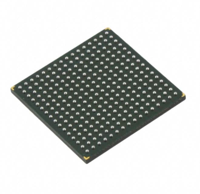
- Part No.:
- 70T651S10BC8
- Manufacturer:
- Renesas
- Category:
- Memory
- Package:
- 256-LBGA
- Datasheet:
-
 70T651S10BC8.pdf
- Description:
- IC SRAM 9MBIT PARALLEL 256CABGA
- Quantity:
- Payment:

- Shipping:

Inventory:2,893
Please send an inquiry. Send us your inquiry, and we will respond immediately.
Product details
Overview
70T651S10BC8 from IDT (now Renesas) is a high-speed 256K × 36-bit asynchronous dual-port static RAM with independent left/right ports, 10 ns max access time (commercial grade), 2.5 V core supply, and selectable 2.5 V/3.3 V I/O interface per port. It enables simultaneous read/write access to the same memory location in telecom switching fabric, network packet buffering, and real-time DSP co-processing systems.
For engineers reviewing the 70T651S10BC8 datasheet, 70T651S10BC8 pinout, 70T651S10BC8 application, or 70T651S10BC8 equivalent, key selection criteria include true dual-port arbitration logic, RapidWrite mode for back-to-back writes, JTAG IEEE 1149.1 compliance, industrial-grade temperature support (–40°C to +85°C), and 256-ball BGA package compatibility with depth/width expansion capability.
Technical Context
The 70T651S10BC8 implements fully asynchronous operation on both ports with on-chip arbitration logic that resolves simultaneous access conflicts via BUSY flag signaling and hardware semaphore support across eight shared flags. Its M/S (Master/Slave) select input configures BUSY as output (Master) or input (Slave), enabling cascaded 72-bit+ memory systems without external logic.
Each port features independent CE0/CE1 chip enables, R/W control, byte-enable lines (BE0–BE3), OPT-selectable I/O voltage (2.5 V or 3.3 V), and sleep mode (ZZL/ZZR) reducing current to ≤10 mA. The device supports RapidWrite mode where address transitions-not R/W pulses-define write cycle boundaries, simplifying high-frequency write sequencing at 100 MHz effective throughput.
Key Specifications
| Parameter | Value and Actual Design Meaning |
|---|---|
| Memory Organization | 256K × 36 bits (9,216 Kbit total); supports 72-bit+ bus width via Master/Slave cascading |
| Access Time (tAA) | 10 ns max (commercial grade); enables 100 MHz sustained random access in synchronous-equivalent systems |
| Core Supply Voltage | 2.5 V ±100 mV; fixed core rail decouples I/O voltage selection from internal logic stability |
| I/O Interface Voltage | Selectable 2.5 V or 3.3 V per port via OPTL/OPTR pins; allows mixed-voltage system integration |
| Operating Temperature | –40°C to +85°C (industrial grade); validated for base station, industrial controller, and avionics edge nodes |
| Package | 256-ball BGA (BC256); 17 mm × 17 mm body, 1.0 mm ball pitch, RoHS-compliant green variant available |
| Standby Current (ISB3) | ≤10 mA (both ports fully disabled, CMOS-level inputs); critical for low-power idle states in always-on infrastructure |
Pinout & Package
70T651S10BC8 is packaged in a 256-ball fine-pitch BGA (BC256) with 17 mm × 17 mm footprint and 1.0 mm ball pitch. Power and ground balls are distributed across the array for low-impedance supply delivery; VDD (2.5 V core) and VDDQ (I/O supply) pins are segregated per port to support independent voltage selection.
| Pin/Terminal | Circuit Role | Design Meaning |
|---|---|---|
| CE0L / CE0R | Chip Enable 0 (Left/Right) | Primary enable; CE0X = VIL and CE1X = VIH activates port X; enables power-down when inactive |
| R/WL / R/WR | Read/Write Control (Left/Right) | Active-low write enable; held low during RapidWrite mode for consecutive address-based writes |
| A0L–A17L / A0R–A17R | Address Inputs (18-bit) | 18-bit address bus per port; A17X is no-connect for 128K variants but functional for 256K configuration |
| I/O0L–I/O35L / I/O0R–I/O35R | Data I/O (36-bit bidirectional) | Two independent 36-bit data buses; byte-enabled (BE0–BE3) for 9-bit granularity writes/reads |
| OPTL / OPTR | I/O Voltage Select (Left/Right) | VDD = 2.5 V → 3.3 V I/O; VSS = 0 V → 2.5 V I/O; sets VDDQL/VDDQR supply requirement |
| ZZL / ZZR | Sleep Mode Input (Left/Right) | Asserted high disables dynamic inputs (except JTAG), reducing current to ≤10 mA per port |
| M/S | Master/Slave Select | VIH = BUSYR/BUSYL output (Master); VIL = BUSYR/BUSYL input (Slave); enables multi-device arbitration |
Key Features
| Feature | Design Value |
|---|---|
| True Dual-Port Architecture | Simultaneous independent read/write access to identical memory locations without external arbitration logic |
| RapidWrite Mode | Eliminates need to toggle R/W between consecutive writes; address transition defines cycle end, easing timing closure at 10 ns |
| Hardware Semaphore Support | Eight dedicated flags accessible via A0–A2 and I/O0; enables inter-processor synchronization without software overhead |
| JTAG Boundary Scan | IEEE 1149.1 compliant TAP controller (TCK/TMS/TDI/TDO/TRST) for production test and debug visibility |
| Flexible I/O Voltage | Per-port OPT pin selects 2.5 V or 3.3 V interface levels-supports legacy 3.3 V controllers interfacing with 2.5 V SoCs |
Applications
| Telecom Switching Fabric | Real-Time DSP Co-Processor Buffer |
|---|---|
|
Use Scenario: High-throughput packet header lookup and forwarding in carrier-grade Ethernet switches. IC Role / Device Role / Timing Role: Dual-port SRAM acts as shared descriptor table between ingress and egress ASICs with sub-10 ns latency. Use Value: Simultaneous access eliminates pipeline stalls; BUSY flag coordination prevents corruption during concurrent updates. |
Use Scenario: Low-latency data exchange between FPGA-based FFT accelerator and ARM Cortex-A9 host processor. IC Role / Device Role / Timing Role: 72-bit-wide memory buffer (two 70T651S10BC8 in Master/Slave) synchronizes streaming sensor data. Use Value: RapidWrite mode sustains 100 MHz write bursts without R/W reassertion, matching FPGA clock domain timing. |
| Industrial PLC Motion Control | Avionics Data Acquisition Hub |
|
Use Scenario: Real-time interpolation table storage and update in servo drive firmware executing at 20 kHz loop rate. IC Role / Device Role / Timing Role: Left port accepts updated trajectory coefficients from ARM core; right port feeds interpolated values to PWM engine. Use Value: Hardware semaphore flags coordinate coefficient swaps atomically-no missed motion cycles due to race conditions. |
Use Scenario: Consolidating analog sensor readings (temperature, pressure, vibration) from multiple aircraft subsystems into a central health monitor. IC Role / Device Role / Timing Role: Dual-port SRAM buffers time-stamped samples from ADC interfaces while host processor performs diagnostics. Use Value: Industrial temperature rating (–40°C to +85°C) and 256-ball BGA ensure reliability in uncontrolled avionics bays. |
Equivalent & Alternatives
The following parts are listed as comparable options for similar dual-port SRAM applications.
| Alternative Part | Technical Difference | Application Difference | Selection Advice |
|---|---|---|---|
| Cypress CY7C1362BV33 | 256K × 36, 10 ns, 3.3 V core + I/O; no OPT-selectable interface; lacks JTAG and RapidWrite | Requires external level shifters for 2.5 V SoC integration; no hardware semaphore or sleep mode | Choose when 3.3 V-only system simplifies power design and JTAG/testability is non-critical |
| Renesas 70V25L25PF8 | 128K × 36, 25 ns, 3.3 V core/I/O; no M/S cascade support; no RapidWrite or semaphore logic | Lower density and speed; suitable only for non-real-time buffering where <50 MHz throughput suffices | Choose only for cost-sensitive legacy designs where 25 ns latency and 128K capacity meet requirements |
Compared with CY7C1362BV33 and 70V25L25PF8, the 70T651S10BC8 uniquely delivers 2.5 V core with per-port I/O voltage flexibility, hardware semaphore arbitration, and RapidWrite mode-enabling higher throughput, lower power, and simpler system-level timing in modern heterogeneous compute architectures.
Availability
70T651S10BC8 is available at Aetrix Electronics and suitable for telecom infrastructure, industrial automation, and aerospace data acquisition requiring stable component supply, long lifecycle support, and RoHS-compliant packaging.
Supply support for 70T651S10BC8 includes scheduled delivery planning, volume procurement assistance, BOM continuity management, traceable sourcing, and lifecycle availability coordination for OEM customers, industrial embedded developers, connected-device designers, and electronics production programs.
Manufacturer
IDT (Integrated Device Technology), now part of Renesas Electronics, specializes in high-performance timing, memory, and interface solutions for communications, computing, and industrial markets.
The 70T651S10BC8 belongs to IDT's high-speed dual-port SRAM product line, engineered for deterministic low-latency memory sharing between heterogeneous processors, FPGAs, and ASICs in real-time embedded systems.
FAQ
What is the maximum operating frequency supported by the 70T651S10BC8?
The 70T651S10BC8 does not operate on a clock signal-it is an asynchronous SRAM. Its 10 ns access time (tAA) supports effective random-access throughput up to 100 MHz in systems where address and control setup/hold times are met. Cycle time (tRC) is also 10 ns, enabling sustained back-to-back operations in RapidWrite mode without intermediate R/W toggling.
Can the left and right ports of the 70T651S10BC8 operate at different I/O voltages?
Yes. The 70T651S10BC8 supports independent I/O voltage selection per port via OPTL and OPTR pins. Setting OPTL = VDD (2.5 V) configures the left port for 3.3 V I/O levels with VDDQL = 3.3 V, while OPTR = VSS (0 V) configures the right port for 2.5 V I/O with VDDQR = 2.5 V-enabling mixed-voltage system integration without level shifters.
How does the RapidWrite mode function in the 70T651S10BC8?
In RapidWrite mode, the 70T651S10BC8 defines write cycle boundaries using address transitions instead of R/W or CE deassertion. R/WL and R/WR can remain low across consecutive writes, eliminating narrow pulse generation. Address stability (tWC = 10 ns), data setup (tDW = 6 ns), and hold (tDH = 0 ns) still apply-but referenced to the ending address edge, simplifying high-speed write sequencing in FPGA or ASIC controllers.
What is the role of the M/S pin in the 70T651S10BC8?
The M/S (Master/Slave) pin configures BUSY flag behavior: when M/S = VIH, BUSYL and BUSYR become outputs indicating local port contention; when M/S = VIL, they become inputs accepting BUSY signals from other devices. This enables daisy-chained arbitration in multi-SRAM systems-e.g., one 70T651S10BC8 as Master coordinates access across three Slave devices in a 108-bit memory bank.
Does the 70T651S10BC8 support JTAG boundary scan, and what pins are required?
Yes, the 70T651S10BC8 fully complies with IEEE 1149.1 JTAG boundary scan. Required pins are TCK (Test Clock), TMS (Test Mode Select), TDI (Test Data In), TDO (Test Data Out), and TRST (Test Reset). These pins remain functional even during ZZ sleep mode, enabling in-system test and debug without disrupting low-power operation.
70T651S10BC8 Specifications
- Product attributes
- Attribute value
- Manufacturer:
- Renesas
- Series:
- -
- Package/Case:
- 256-LBGA
- Packaging:
- Tape & Reel (TR)
- Product Status:
- Obsolete
- Programmable:
- Not Verified
- Memory Type:
- Volatile
- Memory Format:
- SRAM
- Technology:
- SRAM - Dual Port, Asynchronous
- Memory Size:
- 9Mbit
- Memory Organization:
- 256K x 36
- Memory Interface:
- Parallel
- Clock Frequency:
- -
- Write Cycle Time - Word, Page:
- 10ns
- Access Time:
- 10 ns
- Voltage - Supply:
- 2.4V ~ 2.6V
- Operating Temperature:
- 0°C ~ 70°C (TA)
- Grade:
- -
- Qualification:
- -
- Mounting Type:
- Surface Mount
- Supplier Device Package:
- 256-CABGA (17x17)
70T651S10BC8 FAQ
1.How can I place an order for 70T651S10BC8 through Aetrix?
Please submit a Request for Quotation (RFQ) for 70T651S10BC8 on Aetrix. Our sales agent will provide a competitive quotation and guide you through the order confirmation once you accept the terms.
2.Are the price and stock information for 70T651S10BC8 reliable?
The price and inventory of 70T651S10BC8 are updated periodically and may fluctuate due to market conditions. Stock and pricing data are typically refreshed every 24 hours. Quotation validity for 70T651S10BC8 is usually 5 days.
3.What payment methods are accepted for 70T651S10BC8?
We accept Wire Transfer, PayPal, Credit Card, Western Union, MoneyGram, and Escrow for 70T651S10BC8 transactions.
Note: Certain payment methods may incur a processing fee.
4.How is shipping managed for 70T651S10BC8?
70T651S10BC8 orders can be shipped via leading logistics carriers, including DHL, UPS, FedEx, TNT, or Registered Mail.
Once your 70T651S10BC8 order is processed, you will receive an email with the shipment details and tracking number.
Note: Tracking information may take up to 24 hours to appear. Express delivery typically takes 3–5 business days.
5.How can I obtain technical support or documentation for 70T651S10BC8?
For technical support, including 70T651S10BC8 datasheets, pinout diagrams, or application guidance, please contact our engineering support team. They can provide detailed documentation and assistance for your 70T651S10BC8 requirements.
6.How does Aetrix verify that 70T651S10BC8 is sourced from the original manufacturer or authorized distributors?
All 70T651S10BC8 products on Aetrix are procured from qualified distributors and authorized channels. Our dedicated quality assurance team conducts strict verification, including traceability checks and, if necessary, third-party testing. This ensures that 70T651S10BC8 meets industry standards.
7.What is the process for return or replacement of 70T651S10BC8?
All 70T651S10BC8 units undergo pre-shipment inspection (PSI). If there is an issue with 70T651S10BC8, returns or replacements are accepted under the following conditions:
1.Quantity discrepancies, incorrect items, or visible external defects (such as breakage or corrosion), acknowledged by Aetrix.
2.The issue is reported within 90 days of delivery.
3.The 70T651S10BC8 part is unused and in its original packaging.
Return procedure for 70T651S10BC8:
1.Submit a request within 90 days.
2.Obtain a Return Material Authorization (RMA) from Aetrix.
70T651S10BC8 Tags

-
M24C02-WMN6TP
STMicroelectronics

-
AT24C02C-XHM-T
Microchip Technology

-
AT21CS01-STUM10-T
Microchip Technology

-
AT24C02C-SSHM-T
Microchip Technology

-
24LC01BT-I/OT
Microchip Technology

-
M24C02-FMC6TG
STMicroelectronics
-
AT24CS02-SSHM-T
Microchip Technology

-
93LC46BT-I/OT
Microchip Technology
-
AT24C04C-SSHM-T
Microchip Technology

-
24LC01BT-I/SN
Microchip Technology
-
24AA02UIDT-I/OT
Microchip Technology

-
AT24C08C-STUM-T
Microchip Technology
Tech Hub

TTL and CMOS logic families differ in thresholds, loading, output drive, power and timing. This engineering guide compares 74HC and 74HCT, calculates noise margins and checks 3.3 V/5 V compatibility.

A practical engineering guide to 3.3V and 5V logic compatibility, input thresholds, resistor dividers, translator ICs, MOSFET level shifting, I2C pull-ups, timing limits and power-sequencing risks.

The 74HC595 uses push-pull logic outputs, while the TPIC6B595 uses 50 V open-drain DMOS sinks for higher-power loads. This guide compares timing, current limits, 3.3 V interfacing, load wiring, thermal…

The 74HC595 converts serial data into eight stable parallel outputs. This guide covers pin functions, shift and storage timing, OE and MR behavior, drive-current limits, cascading, voltage compatibilit…

A technical comparison of level-sensitive latches and edge-triggered flip-flops, covering timing windows, setup and hold limits, master–slave operation, time borrowing, race-through, HDL inference and…

A D latch stores one bit while Enable controls when data can pass. This reference covers gate-level operation, truth tables, transparency, setup and hold timing, LE versus OE, common ICs and practical …

An SR latch stores one bit through cross-coupled feedback. This engineering reference covers NOR and NAND implementations, truth tables, forbidden-state recovery, gated operation, switch debouncing, fa…

Latch circuits retain one bit through feedback. This technical reference covers SR and D latches, truth tables, transparency, timing limits, latch-versus-flip-flop behavior, applications and common log…

An engineering guide to LED driver operation, constant-current and constant-voltage outputs, linear and switching topologies, dimming, IC selection, calculations, replacement compatibility, and fault c…

Operational amplifier guide covering op amp basics, feedback, ideal vs real op amps, common configurations, buffer circuits, offset, bias current, gain-bandwidth, slew rate, rail-to-rail limits and sel…


