
 My Inquiry
 My Account


Renesas 71V67603S166BQG8
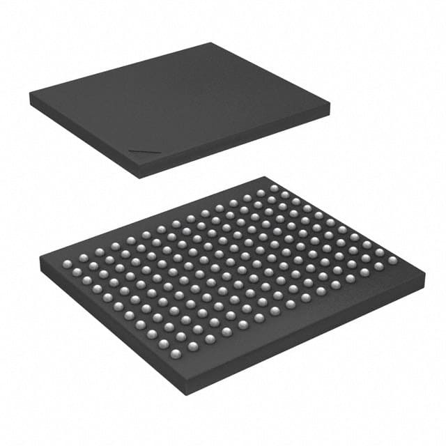
- Part No.:
- 71V67603S166BQG8
- Manufacturer:
- Renesas
- Category:
- Memory
- Package:
- 165-TBGA
- Datasheet:
-
 71V67603S166BQG8.pdf
- Description:
- IC SRAM 9MBIT PARALLEL 165CABGA
- Quantity:
- Payment:

- Shipping:

Inventory:1,277
Please send an inquiry. Send us your inquiry, and we will respond immediately.
Product details
Overview
71V67603S166BQG8 from IDT (now Renesas) is a 256K × 36-bit, 3.3V synchronous SRAM with pipelined outputs, single-cycle deselect, and 166MHz clock operation (3.5ns access time). It supports interleaved/linear burst modes via LBO input, features self-timed write with global/byte write control, and operates across commercial temperature range (0°C to +70°C). It is used in high-speed networking buffers and cache subsystems requiring deterministic low-latency memory access.
For engineers reviewing the 71V67603S166BQG8 datasheet, 71V67603S166BQG8 pinout, 71V67603S166BQG8 application, or 71V67603S166BQG8 equivalent, key selection criteria include burst-mode timing compliance, 3.3V I/O compatibility, TQFP-100 package footprint, ZZ sleep mode power-down behavior, and synchronous CE/CS0/CS1 chip-select logic for multi-chip memory banks.
Technical Context
The 71V67603S166BQG8 implements a synchronous, clock-driven architecture with registered address, data, and control inputs triggered on the rising edge of CLK. Its internal burst counter and pipelined output register enable four consecutive data words per address cycle, with first-word latency of one clock cycle and subsequent words aligned to successive CLK edges.
Burst order is selected statically via LBO (LOW = linear, HIGH = interleaved), and write operations support both global (GW) and byte-level (BW1–BW4) granularity under BWE gating. Power management includes asynchronous ZZ-controlled sleep mode (IZZ ≤ 50mA) and CMOS standby (ISB1 ≤ 50mA), with VDD and VDDQ independently supplied at 3.3V ±5%.
Key Specifications
| Parameter | Value and Actual Design Meaning |
|---|---|
| Memory Organization | 256K × 36-bit (9Mbit); supports 512K × 18-bit configuration via address mapping |
| Clock Frequency | 166MHz max - enables 6ns cycle time with guaranteed 3.5ns clock-to-data (tCD) output valid delay |
| Supply Voltages | VDD = 3.3V ±5% (core), VDDQ = 3.3V ±5% (I/O) - requires dual 3.3V rails with independent decoupling |
| Burst Mode | Configurable linear or interleaved 4-word burst via LBO pin; no external counter needed |
| Write Control | Self-timed write with GW (all bytes) or BW1–BW4 (per 9-bit byte) under BWE synchronization |
| Power-Down | Asynchronous ZZ input reduces supply current to ≤50mA (IZZ) while retaining data |
| Operating Temperature | Commercial grade: 0°C to +70°C - validated for non-extended ambient environments |
Pinout & Package
Packaged in JEDEC-standard 100-pin thin quad flatpack (TQFP), 14mm × 20mm body, lead pitch 0.5mm. Pin 1 marked by corner notch; top-side marking includes "71V67603S166BQG8" and date code.
| Pin/Terminal | Circuit Role | Design Meaning |
|---|---|---|
| A0–A18 | Address Inputs | Synchronous address latching on rising CLK edge when ADSP or ADSC is asserted; A0–A17 used for 256K×36 mode |
| CLK | System Clock Input | Primary timing reference; all synchronous inputs sampled on rising edge; tCH/tCL ≥2.4ns min |
| CE, CS0, CS1 | Chip Enable / Selects | Three-input decode: active when CE=L, CS0=H, CS1=L - enables multi-bank addressing without external logic |
| GW, BWE, BW1–BW4 | Write Control Inputs | GW overrides BWE/BWx; BWE gates BWx; BW1 controls I/O0–7+I/OP1, etc. - enables precise 9-bit byte writes |
| ADV, ADSP, ADSC | Burst Address Control | ADSP/ADSC load initial address; ADV advances internal counter - enables cache-line burst without CPU intervention |
| LBO | Burst Order Select | Static input: LBO=L → linear (00→01→10→11), LBO=H → interleaved (00→01→11→10) - must be stable during operation |
| ZZ | Asynchronous Sleep Mode | High-Z I/O and reduced current (≤50mA) when ZZ=H; no clock required for entry/exit; retains memory contents |
| I/O0–I/O31, I/OP1–I/OP4 | Data I/O (36-bit) | Synchronous bidirectional bus; registered input/output paths; 3.3V-tolerant I/O with VOH≥2.4V, VOL≤0.4V |
Key Features
| Feature | Design Value |
|---|---|
| Pipelined Outputs | First output word available one CLK cycle after address assertion; eliminates wait states in burst-read pipelines |
| Single-Cycle Deselect | Outputs enter high-impedance state within one CLK cycle of chip disable - prevents bus contention in multi-SRAM systems |
| Self-Timed Write Cycle | Internal timing generator eliminates external write-pulse generation; supports variable-length cycles based on GW/BWx setup |
| Linear/Interleaved Burst Selection | LBO pin configures burst address sequence to match CPU/cache controller expectations without firmware change |
| 3.3V Core + I/O Supplies | Dual-rail design allows independent noise isolation between core logic and I/O drivers; meets PCI-X and RISC processor interface requirements |
Applications
| Networking Packet Buffer | Industrial PLC Data Cache |
|---|---|
|
Use Scenario: Storing ingress/egress packet headers and metadata in 10G Ethernet line cards with strict latency budgets. IC Role / Device Role / Timing Role: High-bandwidth, low-latency buffer interfacing directly to MAC-layer logic via synchronous burst reads/writes. Use Value: 166MHz operation delivers 595MB/s sustained throughput; pipelined outputs reduce read turnaround to one clock cycle. |
Use Scenario: Real-time data logging and program execution cache in programmable logic controllers operating in factory-floor environments. IC Role / Device Role / Timing Role: Deterministic-access scratchpad memory for ladder logic execution engine and I/O status shadow registers. Use Value: Single-cycle deselect prevents bus conflicts during rapid task switching; ZZ sleep mode cuts idle power by >85%. |
| Telecom Baseband Processing | Test Equipment Pattern Memory |
|
Use Scenario: Frame buffering in LTE/5G baseband units where burst-aligned data transfer minimizes DMA overhead. IC Role / Device Role / Timing Role: Synchronous SRAM acting as ping-pong buffer between FFT engines and channel encoders. Use Value: Configurable burst order (LBO) matches DSP memory access patterns; 3.3V I/O ensures compatibility with FPGA transceivers. |
Use Scenario: Storing stimulus/response vectors in automated test equipment requiring precise timing alignment and repeatability. IC Role / Device Role / Timing Role: Timing-critical pattern store synchronized to system clock with zero-jitter output registration. Use Value: Guaranteed tCD ≤3.5ns and tOHZ ≤3.5ns ensure sub-nanosecond timing margin for 166MHz pattern rates. |
Equivalent & Alternatives
The following parts are listed as comparable options for similar synchronous SRAM applications.
| Alternative Part | Technical Difference | Application Difference | Selection Advice |
|---|---|---|---|
| CY7C1362BV18-166BZXI | 512K × 18-bit organization; same 166MHz speed, but narrower 18-bit bus; uses different pinout and lacks LBO control | Requires PCB redesign for 18-bit data path; no burst-order flexibility - fixed linear only | Select when system bandwidth demand fits 18-bit interface and burst control is not required. |
| AS7C33128PFS-166BIN | 32M-bit density (1M × 32), 166MHz, but asynchronous OE and no pipelined outputs; higher latency (tAA = 5.5ns) | Cannot replace in burst-intensive designs; unsuitable for cache-like zero-wait-state operation | Consider only for cost-sensitive, non-burst applications where deterministic pipelining is unnecessary. |
Compared with CY7C1362BV18-166BZXI and AS7C33128PFS-166BIN, the 71V67603S166BQG8 uniquely delivers 256K × 36-bit width with configurable burst order and true pipelined output timing - critical for high-efficiency cache and packet-processing subsystems.
Availability
71V67603S166BQG8 is available at Aetrix Electronics and suitable for networking packet buffers, industrial PLC data caches, telecom baseband processing, and test equipment pattern memory requiring stable component supply and long-term obsolescence planning.
Supply support for 71V67603S166BQG8 includes scheduled delivery planning, volume procurement assistance, BOM continuity management, traceable sourcing, and lifecycle availability coordination for OEM customers, industrial embedded developers, connected-device designers, and electronics production programs.
Manufacturer
IDT (Integrated Device Technology), now part of Renesas Electronics, specializes in high-performance timing, memory, and interface ICs for communications, computing, and industrial markets.
The 71V67603S166BQG8 belongs to IDT's high-speed synchronous SRAM product line, designed specifically for low-latency, burst-oriented memory subsystems in network infrastructure and real-time control applications.
FAQ
What is the maximum supported clock frequency for the 71V67603S166BQG8?
The 71V67603S166BQG8 is rated for 166MHz operation with guaranteed 3.5ns clock-to-data (tCD) timing. This corresponds to a minimum clock cycle time (tCYC) of 6ns. Operation at 166MHz is validated across the commercial temperature range (0°C to +70°C) and requires VDD/VDDQ = 3.3V ±5%. Exceeding this frequency violates AC timing specifications and may cause data corruption.
Does the 71V67603S166BQG8 support both linear and interleaved burst modes?
Yes, the 71V67603S166BQG8 supports both linear and interleaved 4-word burst sequences via the LBO (Linear Burst Order) input pin. When LBO is driven LOW, the device executes linear bursts (00→01→10→11); when LBO is HIGH, it executes interleaved bursts (00→01→11→10). LBO is a static input and must remain stable during device operation.
How does the ZZ pin function in the 71V67603S166BQG8?
The ZZ pin on the 71V67603S166BQG8 provides asynchronous entry into full sleep mode. When ZZ is driven HIGH, the device gates its internal clock, disables outputs (high-Z), and reduces supply current to ≤50mA (IZZ) while retaining all stored data. Recovery occurs synchronously on the next rising CLK edge after ZZ returns LOW, with tZZR ≤100ns.
What package type is used for the 71V67603S166BQG8?
The 71V67603S166BQG8 is packaged in a JEDEC-standard 100-pin thin quad flatpack (TQFP) with 14mm × 20mm body size and 0.5mm lead pitch. The suffix "BQG8" explicitly denotes this TQFP-100 package variant. Pin 1 is identified by a corner notch, and the top marking includes "71V67603S166BQG8" followed by date code.
Can the 71V67603S166BQG8 operate with separate VDD and VDDQ supplies?
Yes, the 71V67603S166BQG8 requires two independent 3.3V supplies: VDD (core logic, pins 11, 22, 36, 45, 54, 63, 72, 81, 90) and VDDQ (I/O drivers, pins 47, 56, 65, 74, 83, 92). Both must be regulated to 3.3V ±5%. Separating these rails allows independent decoupling and noise isolation - essential for maintaining signal integrity on the 36-bit I/O bus.
71V67603S166BQG8 Specifications
- Product attributes
- Attribute value
- Manufacturer:
- Renesas
- Series:
- -
- Package/Case:
- 165-TBGA
- Packaging:
- Tape & Reel (TR)
- Product Status:
- Obsolete
- Programmable:
- Not Verified
- Memory Type:
- Volatile
- Memory Format:
- SRAM
- Technology:
- SRAM - Synchronous, SDR
- Memory Size:
- 9Mbit
- Memory Organization:
- 256K x 36
- Memory Interface:
- Parallel
- Clock Frequency:
- 166 MHz
- Write Cycle Time - Word, Page:
- -
- Access Time:
- 3.5 ns
- Voltage - Supply:
- 3.135V ~ 3.465V
- Operating Temperature:
- 0°C ~ 70°C (TA)
- Grade:
- -
- Qualification:
- -
- Mounting Type:
- Surface Mount
- Supplier Device Package:
- 165-CABGA (13x15)
71V67603S166BQG8 FAQ
1.How can I place an order for 71V67603S166BQG8 through Aetrix?
Please submit a Request for Quotation (RFQ) for 71V67603S166BQG8 on Aetrix. Our sales agent will provide a competitive quotation and guide you through the order confirmation once you accept the terms.
2.Are the price and stock information for 71V67603S166BQG8 reliable?
The price and inventory of 71V67603S166BQG8 are updated periodically and may fluctuate due to market conditions. Stock and pricing data are typically refreshed every 24 hours. Quotation validity for 71V67603S166BQG8 is usually 5 days.
3.What payment methods are accepted for 71V67603S166BQG8?
We accept Wire Transfer, PayPal, Credit Card, Western Union, MoneyGram, and Escrow for 71V67603S166BQG8 transactions.
Note: Certain payment methods may incur a processing fee.
4.How is shipping managed for 71V67603S166BQG8?
71V67603S166BQG8 orders can be shipped via leading logistics carriers, including DHL, UPS, FedEx, TNT, or Registered Mail.
Once your 71V67603S166BQG8 order is processed, you will receive an email with the shipment details and tracking number.
Note: Tracking information may take up to 24 hours to appear. Express delivery typically takes 3–5 business days.
5.How can I obtain technical support or documentation for 71V67603S166BQG8?
For technical support, including 71V67603S166BQG8 datasheets, pinout diagrams, or application guidance, please contact our engineering support team. They can provide detailed documentation and assistance for your 71V67603S166BQG8 requirements.
6.How does Aetrix verify that 71V67603S166BQG8 is sourced from the original manufacturer or authorized distributors?
All 71V67603S166BQG8 products on Aetrix are procured from qualified distributors and authorized channels. Our dedicated quality assurance team conducts strict verification, including traceability checks and, if necessary, third-party testing. This ensures that 71V67603S166BQG8 meets industry standards.
7.What is the process for return or replacement of 71V67603S166BQG8?
All 71V67603S166BQG8 units undergo pre-shipment inspection (PSI). If there is an issue with 71V67603S166BQG8, returns or replacements are accepted under the following conditions:
1.Quantity discrepancies, incorrect items, or visible external defects (such as breakage or corrosion), acknowledged by Aetrix.
2.The issue is reported within 90 days of delivery.
3.The 71V67603S166BQG8 part is unused and in its original packaging.
Return procedure for 71V67603S166BQG8:
1.Submit a request within 90 days.
2.Obtain a Return Material Authorization (RMA) from Aetrix.
71V67603S166BQG8 Tags

-
M24C02-WMN6TP
STMicroelectronics

-
AT24C02C-XHM-T
Microchip Technology

-
AT21CS01-STUM10-T
Microchip Technology

-
AT24C02C-SSHM-T
Microchip Technology

-
24LC01BT-I/OT
Microchip Technology

-
M24C02-FMC6TG
STMicroelectronics
-
AT24CS02-SSHM-T
Microchip Technology

-
93LC46BT-I/OT
Microchip Technology
-
AT24C04C-SSHM-T
Microchip Technology

-
24LC01BT-I/SN
Microchip Technology
-
24AA02UIDT-I/OT
Microchip Technology

-
AT24C08C-STUM-T
Microchip Technology
Tech Hub

TTL and CMOS logic families differ in thresholds, loading, output drive, power and timing. This engineering guide compares 74HC and 74HCT, calculates noise margins and checks 3.3 V/5 V compatibility.

A practical engineering guide to 3.3V and 5V logic compatibility, input thresholds, resistor dividers, translator ICs, MOSFET level shifting, I2C pull-ups, timing limits and power-sequencing risks.

The 74HC595 uses push-pull logic outputs, while the TPIC6B595 uses 50 V open-drain DMOS sinks for higher-power loads. This guide compares timing, current limits, 3.3 V interfacing, load wiring, thermal…

The 74HC595 converts serial data into eight stable parallel outputs. This guide covers pin functions, shift and storage timing, OE and MR behavior, drive-current limits, cascading, voltage compatibilit…

A technical comparison of level-sensitive latches and edge-triggered flip-flops, covering timing windows, setup and hold limits, master–slave operation, time borrowing, race-through, HDL inference and…

A D latch stores one bit while Enable controls when data can pass. This reference covers gate-level operation, truth tables, transparency, setup and hold timing, LE versus OE, common ICs and practical …

An SR latch stores one bit through cross-coupled feedback. This engineering reference covers NOR and NAND implementations, truth tables, forbidden-state recovery, gated operation, switch debouncing, fa…

Latch circuits retain one bit through feedback. This technical reference covers SR and D latches, truth tables, transparency, timing limits, latch-versus-flip-flop behavior, applications and common log…

An engineering guide to LED driver operation, constant-current and constant-voltage outputs, linear and switching topologies, dimming, IC selection, calculations, replacement compatibility, and fault c…

Operational amplifier guide covering op amp basics, feedback, ideal vs real op amps, common configurations, buffer circuits, offset, bias current, gain-bandwidth, slew rate, rail-to-rail limits and sel…


