
 My Inquiry
 My Account


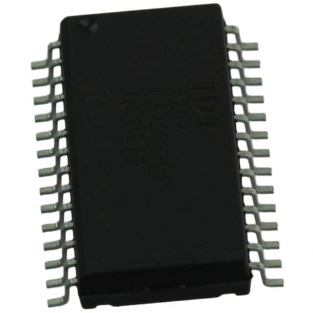
Renesas 7202LA15SOGI
- Part No.:
- 7202LA15SOGI
- Manufacturer:
- Renesas
- Category:
- FIFOs Memory
- Package:
- 28-SOIC (0.345", 8.77mm Width)
- Datasheet:
-
 7202LA15SOGI.pdf
- Description:
- IC FIFO ASYNC 1KX9 15NS 28SOIC
- Quantity:
- Payment:

- Shipping:

Inventory:1,114
Please send an inquiry. Send us your inquiry, and we will respond immediately.
Product details
Overview
7202LA15SOGI from IDT (now Renesas Electronics) is a 1,024 × 9-bit asynchronous CMOS FIFO memory IC used for rate buffering and data flow synchronization between mismatched clock domains or bus protocols. It features 15 ns access time, ultra-low active power (max 440 mW), full/half-full/empty status flags, and auto-retransmit capability. It is deployed in legacy telecom line cards, industrial PLC backplanes, and military avionics data interfaces requiring deterministic latency and MIL-STD-883 Class B compliance.
For engineers reviewing the 7202LA15SOGI datasheet, 7202LA15SOGI pinout, 7202LA15SOGI application, or 7202LA15SOGI equivalent, key selection criteria include its 1,024-word depth, 9-bit width with parity support, 5 V single-supply operation, TSSOP-28 package, and compatibility with depth/width expansion architectures - all critical for legacy system sustainment and FIFO-based protocol bridging.
Technical Context
The 7202LA15SOGI implements a dual-port ring-buffer architecture with independent read/write pointers, eliminating address management overhead. It operates fully asynchronously: write and read cycles are triggered on falling edges of W and R inputs, with no shared clock required.
Status logic generates EF (Empty Flag), FF (Full Flag), and XO/HF (Half-Full Flag) based on pointer arithmetic, enabling real-time buffer occupancy monitoring. Its FL/RT pin supports retransmit mode (resetting read pointer without affecting write pointer), while XI/XO pins enable daisy-chained depth expansion across multiple devices - a feature confirmed for IDT7202LA family members per datasheet Section 9.
Key Specifications
| Parameter | Value and Actual Design Meaning |
|---|---|
| Memory Depth × Width | 1,024 × 9 bits - supports up to 1,024 words of 9-bit data (8 data + 1 parity), sufficient for UART frame buffering or packetized sensor data streams |
| Access Time (tA) | 15 ns max - enables reliable operation at up to 40 MHz effective throughput in high-speed control loops |
| Supply Voltage | 4.5 V to 5.5 V - compatible with legacy 5 V TTL/CMOS logic families and industrial power rails |
| Operating Temperature | –40°C to +85°C - qualified for industrial environments including factory automation and transportation systems |
| Power Consumption | Active: 440 mW max; Power-down: 28 mW max - reduces thermal load in densely packed backplane modules |
| Status Flags | EF, FF, XO/HF - provide hardware-level flow control signals to prevent overflow/underflow without CPU intervention |
| Retransmit Capability | RT input resets read pointer to start - enables repeat transmission of command sequences or firmware blocks without host software overhead |
Pinout & Package
7202LA15SOGI is housed in a 28-pin TSSOP (Thin Shrink Small Outline Package) with 0.65 mm pitch, lead-free (RoHS-compliant) finish, and industrial temperature rating.
| Pin/Terminal | Circuit Role | Design Meaning |
|---|---|---|
| D0–D8 | Data Input Bus | 9-bit parallel input path; supports parity bit insertion for error-checked serial communication links |
| Q0–Q8 | Data Output Bus | Tri-state outputs enabled only during active read cycle (R = LOW); high-impedance otherwise |
| W | Write Enable | Falling-edge-triggered write strobe; initiates storage of D0–D8 into next FIFO location if FF = HIGH |
| R | Read Enable | Falling-edge-triggered read strobe; outputs current Q0–Q8 and advances read pointer if EF = HIGH |
| RS | Reset Input | Active-LOW synchronous reset; forces both read/write pointers to location zero and sets EF = LOW, FF = HIGH |
| FL/RT | First Load / Retransmit | In Single Device Mode (XI = GND): RT function - pulsed LOW resets read pointer to start without altering write pointer |
| XI | Expansion In | GND = Single Device Mode; connected to XO of prior device in Depth Expansion chain |
| XO/HF | Expansion Out / Half-Full Flag | In Single Device Mode: HF output goes LOW when ≥512 locations filled; in Depth Expansion: pulse signal to next device at last location |
| EF | Empty Flag | Open-drain output; LOW indicates no valid data available for read - used to gate R strobes in hardware flow control |
| FF | Full Flag | Open-drain output; LOW indicates no space for new write - used to gate W strobes to prevent overflow |
| VCC, GND | Power Supply | Single 5 V supply; decoupling capacitor required per datasheet layout guidelines to maintain 15 ns timing integrity |
Key Features
| Feature | Design Value |
|---|---|
| Asynchronous Dual-Port Operation | Independent W and R clocks eliminate synchronization logic and metastability risk in multi-domain systems |
| Hardware Flow Control Flags | EF, FF, and HF outputs drive external logic directly - removes need for polling or interrupt-driven buffer management |
| Retransmit Function | RT input enables rapid retransmission of stored command sequences (e.g., SPI register writes or CAN message bursts) without host CPU involvement |
| Expandable Architecture | Depth expansion via XI/XO daisy-chain and width expansion via parallel control lines allow scalable FIFO arrays up to 64k × 9 (per family documentation) |
| MIL-STD-883 Class B Compliance | Qualified for military avionics and ruggedized industrial applications where extended temperature operation and reliability validation are mandatory |
Applications
| Telecom Line Interface | Industrial PLC Backplane |
|---|---|
Use Scenario: Buffering asynchronous HDLC frames between T1/E1 framer and DSP processor in legacy base station equipment. IC Role / Device Role / Timing Role: Asynchronous rate-matching FIFO that absorbs jitter between line-rate clock (1.544 MHz) and internal processing clock (25 MHz). Use Value: Eliminates frame loss during clock domain crossing; 1,024-word depth accommodates worst-case burst latency without software intervention. | Use Scenario: Interfacing Modbus RTU master controller with multiple slave I/O modules over RS-485 bus with variable response times. IC Role / Device Role / Timing Role: Data staging buffer that isolates master polling loop from slave response delays and bus contention. Use Value: Prevents master timeout failures by holding slave replies until polled; EF/FF flags enable hardware handshaking without CPU polling overhead. |
| Military Avionics Data Link | Test Equipment Pattern Generator |
Use Scenario: Storing and retransmitting ARINC 429 word sequences during BIT (Built-In Test) routines in flight control computers. IC Role / Device Role / Timing Role: Deterministic replay buffer with retransmit capability for repeatable test vector delivery. Use Value: RT pin allows instant restart of test sequence upon command - critical for time-critical diagnostics meeting DO-254 Level A requirements. | Use Scenario: Generating high-repetition-rate digital stimulus patterns for ASIC characterization, where pattern length exceeds on-chip memory. IC Role / Device Role / Timing Role: Off-chip pattern store feeding high-speed parallel bus to pattern generator logic. Use Value: 15 ns access time ensures sub-67 MHz pattern update rates; 9-bit width supports 8-bit data + trigger flag for synchronized stimulus events. |
Equivalent & Alternatives
The following parts are listed as comparable options for similar FIFO memory applications.
| Alternative Part | Technical Difference | Application Difference | Selection Advice |
|---|---|---|---|
| 7202LA20SOGI | 20 ns access time (vs. 15 ns); identical 1,024 × 9 organization, TSSOP-28 package, and feature set | Suitable where system timing budget allows 5 ns margin relaxation; lower power consumption in some speed bins | Select when 15 ns timing is not required and cost optimization is prioritized over maximum throughput |
| 7202LA15SOI | Same 15 ns speed grade and 1,024 × 9 spec, but in SOIC-28 package (wider body, 1.27 mm pitch) instead of TSSOP-28 | Better suited for through-hole prototyping or legacy PCBs designed for SOIC footprints | Choose for design reuse in SOIC-based systems or where TSSOP reflow process is unavailable |
Compared with 7202LA15SOGI, the 7202LA20SOGI trades 5 ns speed for potential cost and power advantages, while 7202LA15SOI maintains identical timing but uses a larger SOIC package - making it viable for footprint-compatible upgrades or mixed-technology boards where TSSOP assembly is constrained.
Availability
7202LA15SOGI is available at Aetrix Electronics and suitable for industrial PLC backplanes, telecom line interface modules, and military avionics data links requiring stable component supply for long-lifecycle programs.
Supply support for 7202LA15SOGI includes scheduled delivery planning, volume procurement assistance, BOM continuity management, traceable sourcing, and lifecycle availability coordination for OEM customers, industrial embedded developers, connected-device designers, and electronics production programs.
Manufacturer
IDT (Integrated Device Technology), now part of Renesas Electronics, is a semiconductor company specializing in timing, memory interface, and high-performance interconnect solutions.
The IDT7200L/7201LA/7202LA family was engineered for deterministic, low-latency data buffering in legacy multiprocessing and rate-adaptation systems - targeting applications where asynchronous handshake reliability and MIL-STD-883 qualification outweigh modern integration trends.
FAQ
What is the memory organization of the 7202LA15SOGI?
The 7202LA15SOGI implements a 1,024 × 9-bit first-in/first-out memory array. This means it stores up to 1,024 words, each 9 bits wide - supporting 8-bit data plus 1 parity bit for error detection in serial communications. The architecture uses internal ring pointers, so no external address lines are needed; data is loaded and unloaded strictly in sequential order via W and R control signals. This organization is fixed and cannot be reconfigured.
Does the 7202LA15SOGI support depth expansion, and how is it implemented?
Yes, the 7202LA15SOGI supports depth expansion using its XI (Expansion In) and XO/HF (Expansion Out) pins. In Depth Expansion Mode, multiple 7202LA15SOGI devices are daisy-chained: XO of one device connects to XI of the next. The first device has FL/RT grounded; others hold FL/RT HIGH. External logic must OR all EF and FF outputs to generate composite flags. Critically, the retransmit (RT) and half-full (HF) functions are disabled in this mode - a documented limitation per datasheet Section 9.
What are the voltage and timing requirements for the 7202LA15SOGI reset function?
The 7202LA15SOGI requires an active-LOW reset pulse on the RS pin with minimum width of 15 ns (for 15 ns speed grade) and setup/hold timing relative to W and R inputs. Per datasheet AC specs, tRS = 15 ns min, tRSS = 15 ns setup before rising edge, and tRSR = 10 ns recovery after rising edge. VCC must be within 4.5 V–5.5 V during reset. Upon assertion, RS forces both read and write pointers to location zero, sets EF = LOW and FF = HIGH, and resets HF to HIGH - ensuring deterministic startup state before any read/write activity.
Can the 7202LA15SOGI operate in a read-data-flow-through mode, and what is its latency?
Yes, the 7202LA15SOGI supports read-data-flow-through mode: after writing one word into an empty FIFO, that word becomes readable on the next valid read cycle. Total latency from rising edge of W to valid Q0–Q8 output is tWEF + tA = 15 ns + 15 ns = 30 ns max (per datasheet Figures 17 and AC table). During this window, EF pulses LOW then HIGH, confirming transient emptiness. This mode enables pipelined data transfer without intermediate storage registers - useful in real-time signal processing chains where minimal latency is critical.
Is the 7202LA15SOGI RoHS-compliant, and what is its lead finish?
Yes, the 7202LA15SOGI is RoHS-compliant with lead-free (Pb-free) finish. The "G" suffix in the part number (7202LA15SOGI) explicitly denotes green/RoHS packaging per IDT's ordering guide. This replaces legacy SnPb (tin-lead) versions, which entered EOL with last-time-buy ending June 15, 2018. The device meets JEDEC J-STD-609 Category 1 moisture sensitivity level and is qualified for standard reflow profiles per IPC/JEDEC J-STD-020.
7202LA15SOGI Specifications
- Product attributes
- Attribute value
- Manufacturer:
- Renesas
- Series:
- 7200
- Package/Case:
- 28-SOIC (0.345", 8.77mm Width)
- Packaging:
- Tube
- Product Status:
- Active
- Programmable:
- Not Verified
- Memory Size:
- 9K (1K x 9)
- Function:
- Asynchronous
- Data Rate:
- 40MHz
- Access Time:
- 15ns
- Voltage - Supply:
- 4.5 V ~ 5.5 V
- Current - Supply (Max):
- 80mA
- Bus Directional:
- Uni-Directional
- Expansion Type:
- Depth, Width
- Programmable Flags Support:
- No
- Retransmit Capability:
- Yes
- FWFT Support:
- No
- Operating Temperature:
- -40°C ~ 85°C
- Mounting Type:
- Surface Mount
- Supplier Device Package:
- 28-SOIC
7202LA15SOGI FAQ
1.How can I place an order for 7202LA15SOGI through Aetrix?
Please submit a Request for Quotation (RFQ) for 7202LA15SOGI on Aetrix. Our sales agent will provide a competitive quotation and guide you through the order confirmation once you accept the terms.
2.Are the price and stock information for 7202LA15SOGI reliable?
The price and inventory of 7202LA15SOGI are updated periodically and may fluctuate due to market conditions. Stock and pricing data are typically refreshed every 24 hours. Quotation validity for 7202LA15SOGI is usually 5 days.
3.What payment methods are accepted for 7202LA15SOGI?
We accept Wire Transfer, PayPal, Credit Card, Western Union, MoneyGram, and Escrow for 7202LA15SOGI transactions.
Note: Certain payment methods may incur a processing fee.
4.How is shipping managed for 7202LA15SOGI?
7202LA15SOGI orders can be shipped via leading logistics carriers, including DHL, UPS, FedEx, TNT, or Registered Mail.
Once your 7202LA15SOGI order is processed, you will receive an email with the shipment details and tracking number.
Note: Tracking information may take up to 24 hours to appear. Express delivery typically takes 3–5 business days.
5.How can I obtain technical support or documentation for 7202LA15SOGI?
For technical support, including 7202LA15SOGI datasheets, pinout diagrams, or application guidance, please contact our engineering support team. They can provide detailed documentation and assistance for your 7202LA15SOGI requirements.
6.How does Aetrix verify that 7202LA15SOGI is sourced from the original manufacturer or authorized distributors?
All 7202LA15SOGI products on Aetrix are procured from qualified distributors and authorized channels. Our dedicated quality assurance team conducts strict verification, including traceability checks and, if necessary, third-party testing. This ensures that 7202LA15SOGI meets industry standards.
7.What is the process for return or replacement of 7202LA15SOGI?
All 7202LA15SOGI units undergo pre-shipment inspection (PSI). If there is an issue with 7202LA15SOGI, returns or replacements are accepted under the following conditions:
1.Quantity discrepancies, incorrect items, or visible external defects (such as breakage or corrosion), acknowledged by Aetrix.
2.The issue is reported within 90 days of delivery.
3.The 7202LA15SOGI part is unused and in its original packaging.
Return procedure for 7202LA15SOGI:
1.Submit a request within 90 days.
2.Obtain a Return Material Authorization (RMA) from Aetrix.
7202LA15SOGI Tags
-
7201LA15JGI
Renesas
-
7204L12JG
Renesas

-
72V82L15PAG8
Renesas

-
7205L15JGI
Renesas
-
7208L20JG
Renesas

-
72V2105L10PFG
Renesas
-
72V2111L15PFGI
Renesas

-
72V2113L6PFG
Renesas
-
72V36110L6PFG
Renesas

-
SN74ALVC7804-40DL
Texas Instruments
-
7202LA25JGI
Renesas
-
SN74V245-15PAG
Texas Instruments
Tech Hub

TTL and CMOS logic families differ in thresholds, loading, output drive, power and timing. This engineering guide compares 74HC and 74HCT, calculates noise margins and checks 3.3 V/5 V compatibility.

A practical engineering guide to 3.3V and 5V logic compatibility, input thresholds, resistor dividers, translator ICs, MOSFET level shifting, I2C pull-ups, timing limits and power-sequencing risks.

The 74HC595 uses push-pull logic outputs, while the TPIC6B595 uses 50 V open-drain DMOS sinks for higher-power loads. This guide compares timing, current limits, 3.3 V interfacing, load wiring, thermal…

The 74HC595 converts serial data into eight stable parallel outputs. This guide covers pin functions, shift and storage timing, OE and MR behavior, drive-current limits, cascading, voltage compatibilit…

A technical comparison of level-sensitive latches and edge-triggered flip-flops, covering timing windows, setup and hold limits, master–slave operation, time borrowing, race-through, HDL inference and…

A D latch stores one bit while Enable controls when data can pass. This reference covers gate-level operation, truth tables, transparency, setup and hold timing, LE versus OE, common ICs and practical …

An SR latch stores one bit through cross-coupled feedback. This engineering reference covers NOR and NAND implementations, truth tables, forbidden-state recovery, gated operation, switch debouncing, fa…

Latch circuits retain one bit through feedback. This technical reference covers SR and D latches, truth tables, transparency, timing limits, latch-versus-flip-flop behavior, applications and common log…

An engineering guide to LED driver operation, constant-current and constant-voltage outputs, linear and switching topologies, dimming, IC selection, calculations, replacement compatibility, and fault c…

Operational amplifier guide covering op amp basics, feedback, ideal vs real op amps, common configurations, buffer circuits, offset, bias current, gain-bandwidth, slew rate, rail-to-rail limits and sel…


