
 My Inquiry
 My Account


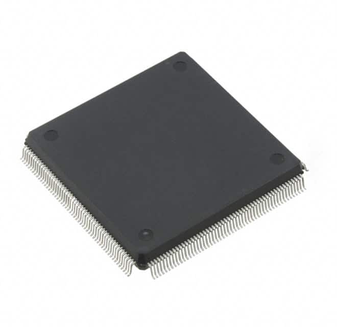
Renesas 72V71660DR
- Part No.:
- 72V71660DR
- Manufacturer:
- Renesas
- Category:
- Signal Switches, Multiplexers, Decoders
- Package:
- 208-BFQFP
- Datasheet:
-
 72V71660DR.pdf
- Description:
- IC MULTIPLEXER 208PQFP
- Quantity:
- Payment:

- Shipping:

Inventory:1,657
Please send an inquiry. Send us your inquiry, and we will respond immediately.
Product details
Overview
IDT72V71660 from Integrated Device Technology is a 3.3 V non-blocking time slot interchange (TSI) digital switch with 16,384 × 16,384 channel capacity at 16.384 Mb/s, 64 serial input/output streams, per-channel variable or constant delay mode selection, automatic ST-BUS®/GCI interface detection, and IEEE-1149.1 JTAG test port - deployed in TDM-based voice switching systems requiring frame-aligned PCM routing.
For engineers reviewing the IDT72V71660 datasheet, IDT72V71660 pinout, IDT72V71660 application, or IDT72V71660 equivalent, key selection considerations include per-stream frame offset programming, microprocessor-accessible connection memory, dual operating modes (Processor vs. Connection), output enable indication capability, and support for industrial temperature range (−40°C to +85°C).
Technical Context
The IDT72V71660 implements a dual-memory architecture: Data Memory stores incoming RX stream data synchronized to an 8 kHz frame pulse (125 μs), while Connection Memory maps output channels to input source addresses or processor-loaded values. Its switching logic supports both Variable Delay Mode (minimum 3 time-slots, optimized for low-latency voice) and Constant Delay Mode (fixed 1-frame + 1-channel latency, preserving frame integrity for wideband data).
Frame alignment is managed via the FE/HCLK pin and WFPS-selectable interface: in ST-BUS® mode, frame evaluation uses falling-edge synchronization; in GCI mode, rising-edge alignment applies. Input skew compensation is enabled through programmable frame offset registers (FOR), supporting ±7.5 clock-cycle adjustments in 0.5-cycle steps per RX stream.
Key Specifications
| Parameter | Value and Actual Design Meaning |
|---|---|
| Switch Capacity | 16,384 × 16,384 non-blocking channels at 16.384 Mb/s; scales to 8,192 × 8,192 at 8.192 Mb/s, 4,096 × 4,096 at 4.096 Mb/s, 2,048 × 2,048 at 2.048 Mb/s |
| Serial I/O Streams | 64 RX inputs and 64 TX outputs, each configurable for 2.048 / 4.096 / 8.192 / 16.384 Mb/s data rates |
| Delay Modes | Per-channel selection: Variable Delay (min. 3 time-slots, latency-optimized) or Constant Delay (1-frame + 1-channel, frame-integrity guaranteed) |
| Microprocessor Interface | 16-bit address (A0–A15) and 16-bit data bus (D0–D15); one-cycle random access to Data Memory, Connection Memory, and control registers |
| Timing Interface Support | Automatic ST-BUS® or GCI bus detection; WFPS pin selects wide-frame pulse (WFPS) or standard frame alignment mode |
| Test & Debug | IEEE-1149.1 JTAG Test Access Port (TCK, TMS, TDI, TDO, TRST) for boundary-scan and internal register access |
| Supply & Environment | +3.3 V ± 0.3 V operation; industrial temperature range −40°C to +85°C; available in 208-pin PBGA (17 mm × 17 mm) and PQFP (28 mm × 28 mm) |
Pinout & Package
Available in two package options: 208-pin Plastic Ball Grid Array (PBGA, 1 mm pitch, 17 mm × 17 mm, order code BB208-1) and 208-pin Plastic Quad Flatpack (PQFP, 0.5 mm pitch, 28 mm × 28 mm, order code DR208-1). Both packages support identical pin functions and electrical specifications.
| Pin/Terminal | Circuit Role | Design Meaning |
|---|---|---|
| CLK | Master serial clock input | Accepts 4.096 / 8.192 / 16.384 MHz; determines bit rate and timing reference for all RX/TX streams |
| RX0–RX63 | Serial data input streams | 64 independent inputs supporting TDM PCM/data; each individually offset-programmable for skew compensation |
| TX0–TX31, TX32/OEI0–TX63/OEI31 | Serial data outputs or output enable indicators | Configurable as 64 TX streams or 32 TX + 32 OEI pins (when OEI=1 in Control Register) |
| ODE | Global output drive enable | When LOW and Output Standby = 0, forces all TX outputs into high-impedance - critical for safe power-up initialization |
| FE/HCLK | Frame evaluation or HCLK input | Mode-dependent: measures input frame skew (FE) or supplies 4.096 MHz clock (HCLK) in WFPS mode |
| WFPS | Wide frame pulse select | LOW = ST-BUS®/GCI auto-detect mode; HIGH = WFPS frame alignment mode (requires external 4.096 MHz HCLK) |
| A0–A15, D0–D15, CS, R/W, DS, DTA | Microprocessor bus interface | Standard RAM-like 16-bit parallel interface enabling direct read/write to internal memories and registers in one cycle |
| TCK, TMS, TDI, TDO, TRST | JTAG test port signals | Full IEEE-1149.1 compliance for boundary-scan testing, debug, and in-system programming |
Key Features
| Feature | Design Value |
|---|---|
| Per-channel delay mode selection | MOD1–MOD0 bits in Connection Memory allow independent assignment of Variable Delay (voice), Constant Delay (data), or Processor Mode per output channel |
| Automatic bus interface detection | Hardware-level recognition of ST-BUS® or GCI framing on FP input eliminates software configuration overhead and reduces setup errors |
| Frame offset measurement & programming | On-chip Frame Evaluation circuitry measures inter-stream skew against FP; results stored in Frame Alignment Register for precise per-RX delay correction |
| Memory block programming | Initialize all Connection Memory locations' upper two bits (MOD1–MOD0) in two frames using BPD1–BPD0 and MBP control bits - accelerates system boot |
| Output enable indication (OEI) | TX32–TX63 pins repurposed as open-drain status indicators (OEI0–OEI31) showing active/high-Z state of corresponding TX0–TX31 outputs |
| Three-state output control hierarchy | Two-level enable: global ODE pin + Output Standby bit override per-channel MOD1–MOD0 settings - ensures fail-safe output isolation during configuration |
Applications
| Voice over TDM Switching | Distributed Telecom Gateway |
|---|---|
Use Scenario: Central office line cards aggregating 64 E1/T1 voice channels into a shared TSI fabric for call routing and conferencing. IC Role / Device Role / Timing Role: Time slot interchange switch performing real-time, non-blocking PCM sample reordering across 64 bidirectional streams. Use Value: Enables sub-100 μs end-to-end voice path latency via Variable Delay Mode while maintaining strict 125 μs frame boundaries required by SS7 and CAS signaling. |
Use Scenario: Multi-shelf telecom gateway where backplane skew between line cards causes misaligned RX frames entering the TSI device. IC Role / Device Role / Timing Role: Skew-compensated TSI switch synchronizing asynchronous input streams before cross-connecting to downstream DSPs or packet processors. Use Value: Per-RX stream frame offset programming (±7.5 CLK cycles @ 16.384 MHz) corrects up to ±460 ns inter-stream skew without external delay lines or FPGA logic. |
| Multi-Protocol TDM Router | Legacy PBX Digital Trunk Interface |
Use Scenario: Enterprise media gateway bridging ST-BUS®-based legacy voice modules with GCI-compliant VoIP processing units. IC Role / Device Role / Timing Role: Protocol-agnostic TSI switch detecting and adapting to ST-BUS® or GCI framing on-the-fly via FP signal analysis. Use Value: Eliminates need for separate interface translation ASICs; single hardware design supports both protocols with no firmware change. |
Use Scenario: Digital trunk card in analog/digital hybrid PBX systems connecting E1 PRI lines to internal time-division multiplexed bus. IC Role / Device Role / Timing Role: High-density TSI switch mapping 30 B-channels and 1 D-channel across multiple E1 spans with per-channel delay tuning. Use Value: 16,384 × 16,384 capacity supports >500 simultaneous voice calls per device; Constant Delay Mode preserves D-channel HDLC frame integrity across switching paths. |
Equivalent & Alternatives
The following parts are listed as comparable options for similar time slot interchange applications.
| Alternative Part | Technical Difference | Application Difference | Selection Advice |
|---|---|---|---|
| IDT72V71260 | 8,192 × 8,192 capacity; supports only 2.048 / 4.096 / 8.192 Mb/s (no 16.384 Mb/s mode); same pinout and register map | Suitable for E1-only systems (< 2.048 Mb/s per stream) or cost-sensitive designs with lower channel count requirements | Select when full 16K×16K bandwidth is unnecessary and board space/cost optimization is prioritized over future scalability. |
| PMC-Sierra PM73120 | 16K×16K TSI with integrated 128-channel HDLC controller; requires external clock synthesis; no JTAG port; different memory-mapped register layout | Better suited for packet-aware TDM gateways needing embedded HDLC framing, but demands more complex driver development and PCB layout | Choose only if HDLC offload and packet-to-TDM bridging are required - not a drop-in replacement due to architectural and interface differences. |
Compared with IDT72V71660, IDT72V71260 offers reduced capacity and data rate support but maintains pin and software compatibility, whereas PM73120 introduces HDLC acceleration at the cost of increased design complexity and loss of JTAG debug visibility.
Availability
IDT72V71660 is available at Aetrix Electronics and suitable for telecom infrastructure, TDM voice switching, and digital trunk interface applications requiring stable component supply, long-term lifecycle assurance, and industrial-grade thermal performance.
Supply support for IDT72V71660 includes scheduled delivery planning, volume procurement assistance, BOM continuity management, traceable sourcing, and lifecycle availability coordination for OEM customers, industrial embedded developers, connected-device designers, and electronics production programs.
Manufacturer
Integrated Device Technology (IDT), now part of Renesas Electronics, specialized in high-performance timing, memory interface, and communications ICs for telecom, computing, and industrial markets.
The IDT72V71660 belongs to IDT's TSI digital switch product line, engineered specifically for non-blocking, low-latency time-slot routing in TDM-based voice and data infrastructure equipment operating across extended temperature ranges.
FAQ
What is the maximum data rate supported by the IDT72V71660?
The IDT72V71660 supports serial data rates of 2.048 Mb/s, 4.096 Mb/s, 8.192 Mb/s, and 16.384 Mb/s on all 64 RX and TX streams. At 16.384 Mb/s, it achieves full 16,384 × 16,384 non-blocking channel capacity with 256 time slots per 125 μs frame. The master clock (CLK) must be set to 16.384 MHz for this rate, and the DR1–DR0 bits in the Control Register must be configured accordingly.
How does the IDT72V71660 handle input stream skew in distributed systems?
The IDT72V71660 compensates for inter-stream skew using its Frame Evaluation feature and Frame Offset Registers (FOR). By asserting the Start Frame Evaluation bit, the device measures delay between the FP input and each RX stream's data edge, storing results in the Frame Alignment Register. These values are then used to program per-RX frame offsets up to +7.5 CLK cycles in 0.5-cycle increments - correcting skew caused by unequal PCB trace lengths or backplane delays.
Can the IDT72V71660 operate in both ST-BUS® and GCI modes simultaneously?
No - the IDT72V71660 automatically detects and locks onto either ST-BUS® or GCI framing based on the FP signal's edge behavior, but operates exclusively in one mode at a time. Mode selection is controlled by the WFPS pin: when LOW, ST-BUS®/GCI auto-detection is active; when HIGH, the device enters Wide Frame Pulse Select (WFPS) mode requiring external 4.096 MHz HCLK and negative frame pulses. It cannot process both formats concurrently.
What is the purpose of the ODE pin on the IDT72V71660?
The ODE (Output Drive Enable) pin provides hardware-level control over all TX output drivers. When ODE is LOW and the Output Standby bit in the Control Register is also LOW, all 64 TX outputs enter high-impedance - a critical safety feature during power-up or reconfiguration. If ODE is HIGH, output drivers are enabled regardless of the Output Standby bit, allowing per-channel control via Connection Memory MOD bits to take precedence.
Does the IDT72V71660 support JTAG boundary-scan testing?
Yes - the IDT72V71660 fully complies with IEEE-1149.1 and includes a dedicated JTAG Test Access Port (TAP) with TCK, TMS, TDI, TDO, and TRST pins. This enables boundary-scan testing of PCB interconnects, in-system register access, and debug visibility into internal memories and control states without requiring external probes or functional test vectors.
72V71660DR Specifications
- Product attributes
- Attribute value
- Manufacturer:
- Renesas
- Series:
- 72V
- Package/Case:
- 208-BFQFP
- Packaging:
- Tray
- Product Status:
- Obsolete
- Type:
- Multiplexer
- Circuit:
- -
- Independent Circuits:
- 4
- Current - Output High, Low:
- -
- Voltage Supply Source:
- Single Supply
- Voltage - Supply:
- 3V ~ 3.6V
- Operating Temperature:
- -40°C ~ 85°C
- Grade:
- -
- Qualification:
- -
- Mounting Type:
- Surface Mount
- Supplier Device Package:
- 208-PQFP (28x28)
72V71660DR FAQ
1.How can I place an order for 72V71660DR through Aetrix?
Please submit a Request for Quotation (RFQ) for 72V71660DR on Aetrix. Our sales agent will provide a competitive quotation and guide you through the order confirmation once you accept the terms.
2.Are the price and stock information for 72V71660DR reliable?
The price and inventory of 72V71660DR are updated periodically and may fluctuate due to market conditions. Stock and pricing data are typically refreshed every 24 hours. Quotation validity for 72V71660DR is usually 5 days.
3.What payment methods are accepted for 72V71660DR?
We accept Wire Transfer, PayPal, Credit Card, Western Union, MoneyGram, and Escrow for 72V71660DR transactions.
Note: Certain payment methods may incur a processing fee.
4.How is shipping managed for 72V71660DR?
72V71660DR orders can be shipped via leading logistics carriers, including DHL, UPS, FedEx, TNT, or Registered Mail.
Once your 72V71660DR order is processed, you will receive an email with the shipment details and tracking number.
Note: Tracking information may take up to 24 hours to appear. Express delivery typically takes 3–5 business days.
5.How can I obtain technical support or documentation for 72V71660DR?
For technical support, including 72V71660DR datasheets, pinout diagrams, or application guidance, please contact our engineering support team. They can provide detailed documentation and assistance for your 72V71660DR requirements.
6.How does Aetrix verify that 72V71660DR is sourced from the original manufacturer or authorized distributors?
All 72V71660DR products on Aetrix are procured from qualified distributors and authorized channels. Our dedicated quality assurance team conducts strict verification, including traceability checks and, if necessary, third-party testing. This ensures that 72V71660DR meets industry standards.
7.What is the process for return or replacement of 72V71660DR?
All 72V71660DR units undergo pre-shipment inspection (PSI). If there is an issue with 72V71660DR, returns or replacements are accepted under the following conditions:
1.Quantity discrepancies, incorrect items, or visible external defects (such as breakage or corrosion), acknowledged by Aetrix.
2.The issue is reported within 90 days of delivery.
3.The 72V71660DR part is unused and in its original packaging.
Return procedure for 72V71660DR:
1.Submit a request within 90 days.
2.Obtain a Return Material Authorization (RMA) from Aetrix.
72V71660DR Tags

-
SN74HC138DR
Texas Instruments
-
TC7SB3157CFU,LF(CT
Toshiba Semiconductor and Storage
-
74CBTLV3257PW,118
Nexperia USA Inc.

-
SN74CBTLV3257PWR
Texas Instruments
-
74CBTLV3257GUX
Nexperia USA Inc.
-
74HC154BQ,118
Nexperia USA Inc.

-
P3S0200GMX
NXP USA Inc.

-
SN74CB3Q3245PWR
Texas Instruments
-
SN74CB3Q3257RGYR
Texas Instruments

-
TCA9543APWR
Texas Instruments
-
TCA9546APWR
Texas Instruments

-
SN74HC138N
Texas Instruments
Tech Hub

TTL and CMOS logic families differ in thresholds, loading, output drive, power and timing. This engineering guide compares 74HC and 74HCT, calculates noise margins and checks 3.3 V/5 V compatibility.

A practical engineering guide to 3.3V and 5V logic compatibility, input thresholds, resistor dividers, translator ICs, MOSFET level shifting, I2C pull-ups, timing limits and power-sequencing risks.

The 74HC595 uses push-pull logic outputs, while the TPIC6B595 uses 50 V open-drain DMOS sinks for higher-power loads. This guide compares timing, current limits, 3.3 V interfacing, load wiring, thermal…

The 74HC595 converts serial data into eight stable parallel outputs. This guide covers pin functions, shift and storage timing, OE and MR behavior, drive-current limits, cascading, voltage compatibilit…

A technical comparison of level-sensitive latches and edge-triggered flip-flops, covering timing windows, setup and hold limits, master–slave operation, time borrowing, race-through, HDL inference and…

A D latch stores one bit while Enable controls when data can pass. This reference covers gate-level operation, truth tables, transparency, setup and hold timing, LE versus OE, common ICs and practical …

An SR latch stores one bit through cross-coupled feedback. This engineering reference covers NOR and NAND implementations, truth tables, forbidden-state recovery, gated operation, switch debouncing, fa…

Latch circuits retain one bit through feedback. This technical reference covers SR and D latches, truth tables, transparency, timing limits, latch-versus-flip-flop behavior, applications and common log…

An engineering guide to LED driver operation, constant-current and constant-voltage outputs, linear and switching topologies, dimming, IC selection, calculations, replacement compatibility, and fault c…

Operational amplifier guide covering op amp basics, feedback, ideal vs real op amps, common configurations, buffer circuits, offset, bias current, gain-bandwidth, slew rate, rail-to-rail limits and sel…


