
 My Inquiry
 My Account


onsemi 74ACT821SPC
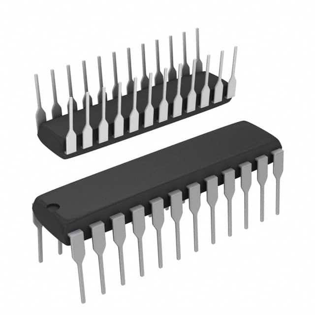
- Part No.:
- 74ACT821SPC
- Manufacturer:
- onsemi
- Category:
- Flip Flops
- Package:
- 24-DIP (0.300", 7.62mm)
- Datasheet:
-
 74ACT821SPC.pdf
- Description:
- IC FF D-TYPE SNGL 10BIT 24DIP
- Quantity:
- Payment:

- Shipping:

Inventory:4,238
Please send an inquiry. Send us your inquiry, and we will respond immediately.
Product details
Overview
74ACT821SPC from Fairchild Semiconductor is a 10-bit edge-triggered D-type flip-flop with noninverting 3-STATE outputs, TTL-compatible inputs, and common clock (CP) and output enable (OE) controls-designed for high-speed bus interfacing in industrial control and data acquisition systems operating at 5V.
For engineers reviewing the 74ACT821SPC datasheet, pinout, applications, or equivalent options, key selection criteria include 5.0V operation, 110 MHz max clock frequency, 24 mA output drive, ±50 mA absolute output current rating, and PDIP-24 package compatibility with legacy through-hole layouts.
Technical Context
The 74ACT821SPC implements ten independent D-type latches triggered on the LOW-to-HIGH transition of a shared buffered clock (CP). Its output enable (OE) input controls all ten outputs simultaneously, placing them in high-impedance state when asserted HIGH without affecting internal flip-flop states.
This device operates strictly within 4.5V–5.5V VCC, meets ACT-series TTL input thresholds (VIH = 2.0V min, VIL = 0.8V max), and delivers guaranteed tPLH/tPHL ≤ 10.5 ns and tPZH/tPHZ ≤ 11.5 ns at 5.0V/CL = 50 pF-enabling reliable synchronization in noise-immune digital backplanes.
Key Specifications
| Parameter | Value and Actual Design Meaning |
|---|---|
| VCC Range | 4.5V to 5.5V - ensures compatibility with standard 5V TTL/CMOS logic rails and eliminates need for level-shifting. |
| Max Clock Frequency | 110 MHz at TA = −40°C to +85°C - supports high-throughput data capture in real-time I/O expansion modules. |
| Output Drive | ±24 mA - provides sufficient sink/source current to directly drive multiple 74-series inputs or LED indicators without buffers. |
| Propagation Delay | tPLH/tPHL ≤ 10.5 ns - enables sub-10 ns timing margins in synchronous bus arbitration circuits. |
| 3-STATE Enable/Disable Time | tPZH/tPHZ ≤ 11.5 ns - allows rapid bus turnaround in time-multiplexed address/data architectures. |
| Input Thresholds | VIH ≥ 2.0V, VIL ≤ 0.8V - guarantees robust noise immunity and direct interface with 5V TTL outputs. |
| Operating Temperature | −40°C to +85°C - qualified for deployment in industrial programmable logic controllers and motor drive control boards. |
Pinout & Package
74ACT821SPC uses a 24-lead Plastic Dual-In-Line Package (PDIP), JEDEC MS-001, 0.300" wide - compatible with standard through-hole prototyping, wave soldering, and legacy socket-based test fixtures.
| Pin/Terminal | Circuit Role | Design Meaning |
|---|---|---|
| 1–10 (D0–D9) | Data Inputs | Asynchronous parallel data inputs synchronized to CP rising edge; meet setup/hold times of tS ≥ 2.0 ns and tH ≥ 2.0 ns. |
| 11 (OE) | Output Enable Input | Active-LOW control: OE = LOW enables outputs; OE = HIGH places O0–O9 in high-impedance state without altering stored data. |
| 12 (GND) | Ground Reference | Primary return path for all logic and output currents; requires low-inductance connection to minimize ground bounce. |
| 13–22 (O0–O9) | Data Outputs | Noninverting, 3-STATE outputs with ±24 mA drive capability; share common OE and CP signals across all ten bits. |
| 23 (CP) | Clock Input | Edge-triggered input: stores Dn values on LOW-to-HIGH transition; internally buffered to reduce skew across ten flip-flops. |
| 24 (VCC) | Supply Voltage | Power supply pin for 4.5V–5.5V operation; decoupling capacitor (0.1 µF ceramic) required adjacent to pin. |
Key Features
| Feature | Design Value |
|---|---|
| 10-bit parallel storage | Simultaneous latching of 10 data lines on single clock edge-ideal for parallel I/O port expansion in microcontroller systems. |
| Common buffered clock (CP) | Minimizes clock skew across all flip-flops, enabling deterministic timing in synchronous data acquisition subsystems. |
| 3-STATE outputs with common OE | Allows bidirectional bus sharing without external tri-state logic; OE assertion does not disturb internal register state. |
| TTL-compatible inputs | Direct interface with legacy 74LS/74F outputs without pull-ups or level translators-reducing BOM count and layout complexity. |
| High-output drive (±24 mA) | Drives up to 10 standard TTL loads or 20 CMOS inputs per output-eliminating need for bus transceivers in moderate-load applications. |
Applications
| Industrial PLC I/O Expansion | Legacy Bus Interface Adapter |
|---|---|
Use Scenario: Adding parallel digital input/output capability to a programmable logic controller using a 5V backplane. IC Role / Device Role / Timing Role: Synchronizes 10-bit sensor status or actuator command data to the PLC's master clock domain while isolating bus loading during idle cycles. Use Value: Enables deterministic sampling of 10 discrete field devices per cycle with <11 ns propagation delay and zero hold-time violation risk. | Use Scenario: Bridging a vintage 8086-based system to modern peripheral modules via a shared 5V data bus. IC Role / Device Role / Timing Role: Acts as a latch and bus driver for 10-bit address or control signals, with OE coordinated to CPU bus grant timing. Use Value: Provides ±24 mA drive and 3-STATE isolation to prevent contention during DMA transfers or interrupt acknowledge cycles. |
| Test Equipment Digital Pattern Generator | Motor Drive Control Register |
Use Scenario: Generating precise, synchronized multi-bit stimulus patterns for functional testing of digital ASICs. IC Role / Device Role / Timing Role: Stores and outputs stable 10-bit test vectors on each clock edge, with OE used to blank outputs during vector transitions. Use Value: Guarantees <10.5 ns output-to-output skew and supports pattern rates up to 110 MHz-meeting IEEE 1149.1 boundary-scan timing requirements. | Use Scenario: Holding PWM duty-cycle and phase-shift settings for a 3-phase inverter in an HVAC variable-frequency drive. IC Role / Device Role / Timing Role: Latches configuration bits from a microcontroller and presents them to gate-driver logic with glitch-free 3-STATE isolation during reprogramming. Use Value: Ensures safe, bounce-free updates of motor control parameters under full load, leveraging OE-controlled output disable before new data is clocked. |
Equivalent & Alternatives
The following parts are listed as comparable options for similar 10-bit D-type latch applications.
| Alternative Part | Technical Difference | Application Difference | Selection Advice |
|---|---|---|---|
| SN74ACT821N | Same logic function, pinout, and AC/DC specs; manufactured by Texas Instruments with identical JEDEC MS-001 PDIP-24 package. | No functional deviation; fully interchangeable in existing 74ACT821SPC designs requiring second-source availability. | Select when TI-sourced parts are preferred for supply chain diversification or long-term lifecycle assurance. |
| 74ACT374PC | Octal (8-bit) version with identical 5V operation, timing, and 3-STATE behavior-but lacks two data bits and uses different pin mapping. | Suitable only where 8-bit width suffices; requires PCB redesign due to different pinout and reduced channel count. | Choose only if system design can accommodate 8-bit data paths and layout revision is feasible. |
Compared with SN74ACT821N and 74ACT374PC, the 74ACT821SPC offers exact 10-bit width and original Fairchild qualification for industrial temperature range-making it optimal for drop-in replacement in legacy PDIP-based control hardware where bit-width and sourcing consistency are critical.
Availability
74ACT821SPC is available at Aetrix Electronics and suitable for industrial PLC I/O expansion, legacy bus interface adapters, and test equipment digital pattern generators requiring stable component supply and long-term obsolescence management.
Supply support for 74ACT821SPC includes scheduled delivery planning, volume procurement assistance, BOM continuity management, traceable sourcing, and lifecycle availability coordination for OEM customers, industrial embedded developers, connected-device designers, and electronics production programs.
Manufacturer
Fairchild Semiconductor was a U.S.-based semiconductor company specializing in analog and mixed-signal ICs, acquired by ON Semiconductor in 2016; its legacy logic portfolio remains widely deployed in industrial and automotive systems.
The 74ACT821SPC belongs to Fairchild's ACT (Advanced CMOS TTL-compatible) logic family-designed specifically for high-speed, low-power 5V digital systems requiring robust noise immunity and direct TTL interoperability.
FAQ
What is the maximum operating voltage for the 74ACT821SPC?
The 74ACT821SPC has a specified VCC operating range of 4.5V to 5.5V. Operation outside this window is not guaranteed and may cause timing violations or increased ICC. Absolute maximum rating is 7.0V, but sustained use above 5.5V risks permanent damage and invalidates parametric guarantees per the datasheet.
Does the 74ACT821SPC support hot insertion or live insertion into a powered bus?
No, the 74ACT821SPC is not designed for hot insertion. Its absolute maximum ratings specify DC input diode current limits of ±20 mA, and no hot-swap protection circuitry is integrated. Applying signal or power before VCC stabilization may forward-bias input clamps and exceed IOK limits, risking latch-up or degradation.
Can the 74ACT821SPC be used with a 3.3V microcontroller interface?
No-the 74ACT821SPC requires 4.5V–5.5V VCC and is not 3.3V-tolerant. Its VIH minimum is 2.0V, but driving inputs from a 3.3V system violates VCC–VIH margin requirements and risks undefined output behavior. A level-shifter or 5V-compatible MCU is required for reliable operation.
What is the purpose of the broadside pinout in the 74ACT821SPC PDIP package?
The broadside pinout places D0–D9 on one side (pins 1–10) and O0–O9 on the opposite side (pins 13–22), minimizing trace crossovers in PCB layout. This arrangement simplifies routing for parallel bus applications and reduces capacitive coupling between input and output nets-critical for maintaining signal integrity at >100 MHz clock rates.
Is the 74ACT821SPC RoHS compliant?
Yes, the 74ACT821SPC is RoHS compliant per the original Fairchild specification and ON Semiconductor's post-acquisition compliance documentation. It contains no lead in excess of 0.1% by weight in homogeneous materials and meets EU Directive 2011/65/EU Annex II exemptions applicable to legacy logic devices.
74ACT821SPC Specifications
- Product attributes
- Attribute value
- Manufacturer:
- onsemi
- Series:
- 74ACT
- Package/Case:
- 24-DIP (0.300", 7.62mm)
- Packaging:
- Tube
- Product Status:
- Obsolete
- Function:
- Standard
- Type:
- D-Type
- Output Type:
- Tri-State, Non-Inverted
- Number of Elements:
- 1
- Number of Bits per Element:
- 10
- Clock Frequency:
- 150 MHz
- Max Propagation Delay @ V, Max CL:
- 9.5ns @ 5V, 50pF
- Trigger Type:
- Positive Edge
- Current - Output High, Low:
- 24mA, 24mA
- Voltage - Supply:
- 4.5V ~ 5.5V
- Current - Quiescent (Iq):
- 80 µA
- Input Capacitance:
- 4.5 pF
- Operating Temperature:
- -40°C ~ 85°C (TA)
- Grade:
- -
- Qualification:
- -
- Mounting Type:
- Through Hole
- Supplier Device Package:
- 24-PDIP
74ACT821SPC FAQ
1.How can I place an order for 74ACT821SPC through Aetrix?
Please submit a Request for Quotation (RFQ) for 74ACT821SPC on Aetrix. Our sales agent will provide a competitive quotation and guide you through the order confirmation once you accept the terms.
2.Are the price and stock information for 74ACT821SPC reliable?
The price and inventory of 74ACT821SPC are updated periodically and may fluctuate due to market conditions. Stock and pricing data are typically refreshed every 24 hours. Quotation validity for 74ACT821SPC is usually 5 days.
3.What payment methods are accepted for 74ACT821SPC?
We accept Wire Transfer, PayPal, Credit Card, Western Union, MoneyGram, and Escrow for 74ACT821SPC transactions.
Note: Certain payment methods may incur a processing fee.
4.How is shipping managed for 74ACT821SPC?
74ACT821SPC orders can be shipped via leading logistics carriers, including DHL, UPS, FedEx, TNT, or Registered Mail.
Once your 74ACT821SPC order is processed, you will receive an email with the shipment details and tracking number.
Note: Tracking information may take up to 24 hours to appear. Express delivery typically takes 3–5 business days.
5.How can I obtain technical support or documentation for 74ACT821SPC?
For technical support, including 74ACT821SPC datasheets, pinout diagrams, or application guidance, please contact our engineering support team. They can provide detailed documentation and assistance for your 74ACT821SPC requirements.
6.How does Aetrix verify that 74ACT821SPC is sourced from the original manufacturer or authorized distributors?
All 74ACT821SPC products on Aetrix are procured from qualified distributors and authorized channels. Our dedicated quality assurance team conducts strict verification, including traceability checks and, if necessary, third-party testing. This ensures that 74ACT821SPC meets industry standards.
7.What is the process for return or replacement of 74ACT821SPC?
All 74ACT821SPC units undergo pre-shipment inspection (PSI). If there is an issue with 74ACT821SPC, returns or replacements are accepted under the following conditions:
1.Quantity discrepancies, incorrect items, or visible external defects (such as breakage or corrosion), acknowledged by Aetrix.
2.The issue is reported within 90 days of delivery.
3.The 74ACT821SPC part is unused and in its original packaging.
Return procedure for 74ACT821SPC:
1.Submit a request within 90 days.
2.Obtain a Return Material Authorization (RMA) from Aetrix.
74ACT821SPC Tags

-
SN74HC74DR
Texas Instruments

-
SN74HC74PWR
Texas Instruments
-
74LVC1G74GT,115
Nexperia USA Inc.

-
SN74LVC2G74DCUR
Texas Instruments
-
CD4013BM96
Texas Instruments

-
SN74HCT273PWR
Texas Instruments
-
SN74LVC1G74DCUR
Texas Instruments
-
SN74HC574DWR
Texas Instruments
-
74LVC1G74DC,125
Nexperia USA Inc.
-
SN74HC273DWR
Texas Instruments
-
SN74HCT574DWR
Texas Instruments
-
SN74LVC1G74DCTR
Texas Instruments
Tech Hub

Counterfeit components can hide behind convincing markings and passing basic function tests. This engineering reference covers source traceability, external inspection, X-ray, XRF, electrical testing, …

A practical engineering and sourcing framework covering lifecycle verification, lifetime-buy calculations, replacement qualification, supplier checks and counterfeit-risk controls.

TTL and CMOS logic families differ in thresholds, loading, output drive, power and timing. This engineering guide compares 74HC and 74HCT, calculates noise margins and checks 3.3 V/5 V compatibility.

A practical engineering guide to 3.3V and 5V logic compatibility, input thresholds, resistor dividers, translator ICs, MOSFET level shifting, I2C pull-ups, timing limits and power-sequencing risks.

The 74HC595 uses push-pull logic outputs, while the TPIC6B595 uses 50 V open-drain DMOS sinks for higher-power loads. This guide compares timing, current limits, 3.3 V interfacing, load wiring, thermal…

The 74HC595 converts serial data into eight stable parallel outputs. This guide covers pin functions, shift and storage timing, OE and MR behavior, drive-current limits, cascading, voltage compatibilit…

A technical comparison of level-sensitive latches and edge-triggered flip-flops, covering timing windows, setup and hold limits, master–slave operation, time borrowing, race-through, HDL inference and…

A D latch stores one bit while Enable controls when data can pass. This reference covers gate-level operation, truth tables, transparency, setup and hold timing, LE versus OE, common ICs and practical …

An SR latch stores one bit through cross-coupled feedback. This engineering reference covers NOR and NAND implementations, truth tables, forbidden-state recovery, gated operation, switch debouncing, fa…

Latch circuits retain one bit through feedback. This technical reference covers SR and D latches, truth tables, transparency, timing limits, latch-versus-flip-flop behavior, applications and common log…


