
 My Inquiry
 My Account


NXP Semiconductors 74HCT03DB,112
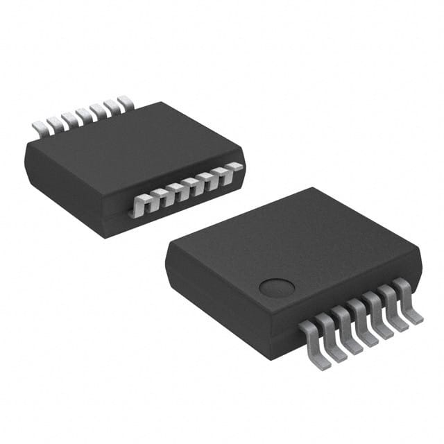
- Part No.:
- 74HCT03DB,112
- Manufacturer:
- NXP Semiconductors
- Category:
- Gates and Inverters
- Package:
- 14-SSOP (0.209", 5.30mm Width)
- Datasheet:
-
 74HCT03DB,112.pdf
- Description:
- IC GATE NAND 4CH 2-INP 14-SSOP
- Quantity:
- Payment:

- Shipping:

Inventory:3,276
Please send an inquiry. Send us your inquiry, and we will respond immediately.
Product details
Overview
74HCT03DB,112 from Nexperia USA Inc. is a quad 2-input NAND gate with open-drain outputs in SSOP package. Its compatibility depends on logic family, threshold behavior, output structure, timing, and control pins rather than package code alone.
74HCT03DB,112 is most relevant to logic-level translation, control-signal buffering, timing and counter logic, embedded interface glue logic, where the surrounding circuit depends on the same rating profile, footprint, thermal behavior, and sourcing continuity.
Technical Context
74HCT03DB,112 is a logic-family IC whose real compatibility depends on supply range, input thresholds, output structure, timing, and pinout. Package suffixes can change assembly without changing the logic name.
For glue logic and interface paths, 74HCT03DB,112 must be matched to the surrounding voltage domain. Enable pins, open-drain outputs, Schmitt inputs, counters, or latches can change system behavior if substituted loosely.
Key Specifications
| Parameter | Value and Actual Design Meaning |
|---|---|
| Device Type | quad 2-input NAND gate with open-drain outputs for logic-level translation and control-signal buffering. |
| Technology | Nexperia CMOS logic family technology |
| Voltage Rating / Operating Class | 5 V logic-family supply class |
| Current / Output Class | logic output-drive current class |
| Package | SSOP package |
| Primary Circuit Role | Provides the board-level function indicated by its family code while preserving package-specific assembly constraints. |
| Thermal Design Meaning | Power loss and temperature rise should be reviewed using the real waveform, package mounting, and board layout. |
| Assembly Meaning | The package code affects pick-and-place setup, solder-joint inspection, and mechanical compatibility on existing boards. |
| Design Detail | standard Nexperia logic ordering |
| Design Detail | controlled input thresholds |
| Design Detail | high-speed CMOS switching |
Pinout & Package
74HCT03DB,112 uses SSOP package. Pin mapping, polarity, or item format should be matched to the exact board, fixture, or procurement requirement before replacement.
| Pin / Terminal | Circuit Role | Design Meaning |
|---|---|---|
| VCC and GND | Logic supply and ground pins. | Set the voltage domain, input thresholds, and output swing. |
| Input pins | Receive logic, clock, select, trigger, or direction signals. | Input type and threshold family must match the driving device. |
| Output / control pins | Drive the next logic stage, bus, latch, counter, or protected output. | Output enable, open-drain, or 3-state behavior must match the schematic. |
Key Features
- 74HCT03DB,112 is identified as a quad 2-input NAND gate with open-drain outputs.
- 5 V logic-family supply class voltage or operating class for the relevant circuit stress.
- logic output-drive current class current or output class, subject to package and thermal derating.
- SSOP package package or item format for procurement and assembly review.
- standard Nexperia logic ordering
- controlled input thresholds
- high-speed CMOS switching
- Logic-family thresholds and output behavior must match the system voltage domain.
- Control pins such as enable, direction, trigger, or reset require schematic-level review.
Applications
| logic-level translation | control-signal buffering |
|---|---|
|
Use Scenario: logic-level translation where the design needs 5 V logic-family supply class behavior from 74HCT03DB,112. Device Role: 74HCT03DB,112 provides the quad 2-input NAND gate with open-drain outputs function in the local circuit block. Use Value: The part keeps the SSOP package footprint and rating profile aligned with the intended board function. |
Use Scenario: control-signal buffering requiring the device family behavior instead of a generic component choice. Device Role: 74HCT03DB,112 handles the switching, protection, control, memory, or power-path task defined by its category. Use Value: Using the correct family reduces requalification risk around timing, voltage, current, thermal, and package constraints. |
| timing and counter logic | embedded interface glue logic |
|
Use Scenario: timing and counter logic where operating stress, package size, and sourcing continuity all matter. Device Role: 74HCT03DB,112 sits in the circuit as a BOM-controlled part rather than a cosmetic ordering code. Use Value: The device-specific rating and package information help engineers avoid unsuitable substitutions during procurement. |
Use Scenario: embedded interface glue logic for legacy, current-production, or lifecycle-sensitive assemblies. Device Role: 74HCT03DB,112 supports the same product-family function when matched to the existing schematic and layout. Use Value: A careful match protects system behavior while giving buyers a traceable sourcing path. |
Equivalent & Alternatives
When evaluating 74HCT03DB,112 equivalent devices, compare voltage rating or operating class, current or output capability, package and footprint, pin mapping or polarity, thermal behavior, qualification suffix, lifecycle and sourcing status. A similar family name is not enough when the board depends on timing, leakage, firmware, optical output, or protection behavior.
| Alternative Part | Technical Difference | Application Difference | Selection Advice |
|---|---|---|---|
| 74HCT03DB | Same base family identifier with ordering, reel, compliance, or package suffix differences from 74HCT03DB,112. | Useful when the electrical identity is intended to remain close but procurement format differs. | Check package drawing, marking, suffix, qualification status, and approved-source rules before selection. |
| 74HCT03DB | Same Nexperia logic-family base code without the full packing suffix of 74HCT03DB,112. | Appropriate only when package, temperature grade, and automotive suffix remain acceptable. | Compare logic family, pinout, output type, enable polarity, supply range, and package code. |
Quality
74HCT03DB,112 should be sourced as original Nexperia USA Inc. material through traceable and controlled supply channels. Quality verification may include logic input/output testing, supply-current screening, package coplanarity inspection, marking review, and reel label verification, along with incoming inspection suited to quad 2-input NAND gate with open-drain outputs production, repair, or lifecycle procurement.
Availability
74HCT03DB,112 is available at Aetrix Electronics and suitable for logic-level translation, control-signal buffering, timing and counter logic, embedded interface glue logic requiring 5 V logic-family supply class, SSOP package in a controlled BOM or repair program.
Supply support may include scheduled delivery planning, volume procurement support, BOM continuity assistance, traceable sourcing management, and lifecycle availability coordination for manufacturers, repair teams, contract manufacturers, and engineering buyers managing quad 2-input NAND gate with open-drain outputs demand.
For production deployment, confirming package fit, pin mapping or polarity, electrical rating, temperature margin, lifecycle status, approved manufacturer identity, and sourcing continuity helps reduce qualification risk for 74HCT03DB,112.
Manufacturer
Nexperia USA Inc. supplies logic ICs, ESD protection, bipolar transistors, MOSFETs, diodes, rectifiers, and small-signal discrete semiconductors for automotive, industrial, mobile, and consumer electronics. 74HCT03DB,112 belongs to the Nexperia product area indicated by its family prefix.
FAQ
What is 74HCT03DB,112 used for?
74HCT03DB,112 is used for logic-level translation, control-signal buffering, timing and counter logic. In those circuits, 74HCT03DB,112 provides the quad 2-input NAND gate with open-drain outputs function with 5 V logic-family supply class, SSOP package. The final selection should match the schematic role, operating stress, package footprint, and sourcing requirements.
What logic family details matter for 74HCT03DB,112?
74HCT03DB,112 must match the intended logic family, supply range, input thresholds, output structure, timing, and package pinout. For 74HCT03DB,112, a different 74-series suffix can change package, automotive grade, or control behavior even when the broad function looks similar.
What should be checked in the 74HCT03DB,112 pinout?
The 74HCT03DB,112 pinout should be checked for VCC, GND, input pins, output pins, enables, direction controls, triggers, or latch controls depending on the function. Incorrect pin mapping on 74HCT03DB,112 can cause bus contention, stuck outputs, or timing faults.
Can 74HCT03DB,112 be replaced by a similar part?
74HCT03DB,112 can be compared with similar family members only after electrical limits, package, orientation, qualification suffix, timing or leakage behavior, and approved-source rules are reviewed. A similar name alone is not enough because 74HCT03DB,112 may carry package, program, bin, or lifecycle details.
Why source 74HCT03DB,112 through Aetrix Electronics?
Sourcing 74HCT03DB,112 through Aetrix Electronics supports traceable procurement, scheduled delivery planning, BOM continuity assistance, and lifecycle availability coordination. This is useful when 74HCT03DB,112 is needed for production builds, repair lots, controlled alternates, or long-running equipment support.
74HCT03DB,112 Specifications
- Product attributes
- Attribute value
- Manufacturer:
- NXP Semiconductors
- Series:
- 74HCT
- Package/Case:
- 14-SSOP (0.209", 5.30mm Width)
- Packaging:
- Tube
- Product Status:
- Active
- Logic Type:
- NAND Gate
- Number of Circuits:
- 4
- Number of Inputs:
- 2
- Features:
- Open Drain
- Voltage - Supply:
- 4.5V ~ 5.5V
- Current - Quiescent (Max):
- 2 µA
- Current - Output High, Low:
- -, 4mA
- Input Logic Level - Low:
- 0.8V
- Input Logic Level - High:
- 2V
- Max Propagation Delay @ V, Max CL:
- 24ns @ 4.5V, 50pF
- Operating Temperature:
- -40°C ~ 125°C
- Grade:
- -
- Qualification:
- -
- Mounting Type:
- Surface Mount
- Supplier Device Package:
- 14-SSOP
74HCT03DB,112 FAQ
1.How can I place an order for 74HCT03DB,112 through Aetrix?
Please submit a Request for Quotation (RFQ) for 74HCT03DB,112 on Aetrix. Our sales agent will provide a competitive quotation and guide you through the order confirmation once you accept the terms.
2.Are the price and stock information for 74HCT03DB,112 reliable?
The price and inventory of 74HCT03DB,112 are updated periodically and may fluctuate due to market conditions. Stock and pricing data are typically refreshed every 24 hours. Quotation validity for 74HCT03DB,112 is usually 5 days.
3.What payment methods are accepted for 74HCT03DB,112?
We accept Wire Transfer, PayPal, Credit Card, Western Union, MoneyGram, and Escrow for 74HCT03DB,112 transactions.
Note: Certain payment methods may incur a processing fee.
4.How is shipping managed for 74HCT03DB,112?
74HCT03DB,112 orders can be shipped via leading logistics carriers, including DHL, UPS, FedEx, TNT, or Registered Mail.
Once your 74HCT03DB,112 order is processed, you will receive an email with the shipment details and tracking number.
Note: Tracking information may take up to 24 hours to appear. Express delivery typically takes 3–5 business days.
5.How can I obtain technical support or documentation for 74HCT03DB,112?
For technical support, including 74HCT03DB,112 datasheets, pinout diagrams, or application guidance, please contact our engineering support team. They can provide detailed documentation and assistance for your 74HCT03DB,112 requirements.
6.How does Aetrix verify that 74HCT03DB,112 is sourced from the original manufacturer or authorized distributors?
All 74HCT03DB,112 products on Aetrix are procured from qualified distributors and authorized channels. Our dedicated quality assurance team conducts strict verification, including traceability checks and, if necessary, third-party testing. This ensures that 74HCT03DB,112 meets industry standards.
7.What is the process for return or replacement of 74HCT03DB,112?
All 74HCT03DB,112 units undergo pre-shipment inspection (PSI). If there is an issue with 74HCT03DB,112, returns or replacements are accepted under the following conditions:
1.Quantity discrepancies, incorrect items, or visible external defects (such as breakage or corrosion), acknowledged by Aetrix.
2.The issue is reported within 90 days of delivery.
3.The 74HCT03DB,112 part is unused and in its original packaging.
Return procedure for 74HCT03DB,112:
1.Submit a request within 90 days.
2.Obtain a Return Material Authorization (RMA) from Aetrix.
74HCT03DB,112 Tags

-
SN74LVC1G14DBVR
Texas Instruments

-
SN74LVC1G14DCKR
Texas Instruments
-
SN74AHC1G14DBVR
Texas Instruments
-
SN74LVC1G08DBVR
Texas Instruments
-
SN74LVC1G08DCKR
Texas Instruments
-
SN74LVC1G32DCKR
Texas Instruments
-
SN74LVC1G04DBVR
Texas Instruments
.jpg)
-
74LVC1G08GW,125
Nexperia USA Inc.
-
SN74LVC1G04DCKR
Texas Instruments
-
SN74AHC1G08DBVR
Texas Instruments
-
SN74LVC1G32DBVR
Texas Instruments
-
SN74AHCT1G08DBVR
Texas Instruments
Tech Hub

An engineering guide to LED driver operation, constant-current and constant-voltage outputs, linear and switching topologies, dimming, IC selection, calculations, replacement compatibility, and fault c…

Operational amplifier guide covering op amp basics, feedback, ideal vs real op amps, common configurations, buffer circuits, offset, bias current, gain-bandwidth, slew rate, rail-to-rail limits and sel…

Jumper cables guide covering safe connection order, red and black clamp placement, final ground connection, cable gauge, length, clamp quality, copper vs CCA cables, jump starter comparison and battery…

LDO regulator guide covering low dropout voltage, power dissipation, thermal design, PSRR, output noise, capacitor stability, adjustable LDO circuits, LDO vs buck converter and datasheet selection chec…

Conditional Access Module guide covering CAM meaning, CI/CI+ interface, smart card authorization, DVB security workflow, TV and set-top box compatibility, internal electronics, ESD protection, connecto…

Guide to electronic component obsolescence covering EOL risk, PCN/PDN notices, last-time buy planning, replacement options, form-fit-function validation, counterfeit risk and BOM lifecycle management.

18650 battery guide covering lithium-ion cell basics, 3.6V/3.7V voltage, 4.2V charging, mAh and Wh capacity, protected cells, chargers, BMS, series-parallel packs, holders, welding and sourcing checks.…

Hall effect sensor guide covering working principle, linear and digital sensors, Arduino circuits, current sensing, speed detection, automotive applications, A3144 examples, signal filtering and datash…

Product Change Notification guide for electronic components, covering PCN meaning, PCN vs PDN/EOL, common change types, risk levels, form-fit-function review, engineering validation, BOM control, LTB/L…

A practical guide to blend door actuators, covering HVAC function, symptoms, location, AC and heater issues, reset and calibration, replacement cost, electrical diagnosis, compatibility checks, and rep…


