
 My Inquiry
 My Account


Nexperia USA Inc. 74HCT165PW,112

- Part No.:
- 74HCT165PW,112
- Manufacturer:
- Nexperia USA Inc.
- Category:
- Shift Registers
- Package:
- 16-TSSOP (0.173", 4.40mm Width)
- Datasheet:
-
 74HCT165PW,112.pdf
- Description:
- IC SHIFT REG 8BIT PI-SO 16TSSOP
- Quantity:
- Payment:

- Shipping:

Inventory:4,186
Please send an inquiry. Send us your inquiry, and we will respond immediately.
Product details
Overview
74HCT165PW,112 from Nexperia is an 8-bit parallel-in/serial-out shift register with TTL-compatible inputs, asynchronous parallel load (PL), synchronous serial shift (CP/CE), complementary Q7/Q7 outputs, and operation from 4.5 V to 5.5 V across –40 °C to +125 °C. It enables parallel data capture from microcontroller GPIO banks or sensor arrays followed by compact serial transmission over SPI or UART interfaces.
For engineers reviewing the 74HCT165PW,112 datasheet, 74HCT165PW,112 pinout, 74HCT165PW,112 application, or 74HCT165PW,112 equivalent, this device serves as a low-power, temperature-stable interface for expanding digital I/O in industrial control panels, automotive body controllers, and embedded data acquisition systems where level-shifted input tolerance and deterministic timing are required.
Technical Context
The 74HCT165PW,112 implements a synchronous 8-stage shift register with dual-path output buffering: Q7 provides the MSB of the shifted-out data stream, while Q7 delivers its logical complement. Its asynchronous PL input allows immediate latching of parallel inputs D0–D7 without clock dependency, enabling precise sampling of external signals on demand.
Operation is governed by edge-triggered CP (LOW-to-HIGH) and active-low CE gating - when CE is HIGH, CP transitions are ignored, halting shift activity. Input clamping supports 15 V overvoltage tolerance, permitting direct interfacing with 5 V logic driving 3.3 V microcontrollers without external level-shifting components.
Key Specifications
| Parameter | Value and Actual Design Meaning |
|---|---|
| Supply Voltage | 4.5 V to 5.5 V - ensures compatibility with standard 5 V logic rails and stable operation under industrial supply ripple. |
| Input Logic Type | TTL-level - accepts 2.0 V minimum VIH and 0.8 V maximum VIL, enabling direct connection to legacy 5 V MCU peripherals. |
| Propagation Delay (tpd) | 14 ns to 51 ns (VCC = 4.5 V) - guarantees sub-50 ns timing margin for 10 MHz serial clocking in real-time control loops. |
| Operating Temperature | –40 °C to +125 °C - qualified for under-hood automotive and factory-floor industrial environments without derating. |
| Output Drive Strength | ±4.0 mA (VOH/VOL @ VCC = 4.5 V) - sufficient to drive multiple CMOS inputs or short PCB traces without fanout limitation. |
| Power Dissipation | Max 160 μA ICC (VCC = 6.0 V, –40 °C to +125 °C) - enables battery-powered or thermally constrained designs with minimal quiescent load. |
| ESD Rating | HBM > 2000 V, CDM > 1000 V - meets IEC 61000-4-2 Level 2 requirements for robust handling in manufacturing and field service. |
Pinout & Package
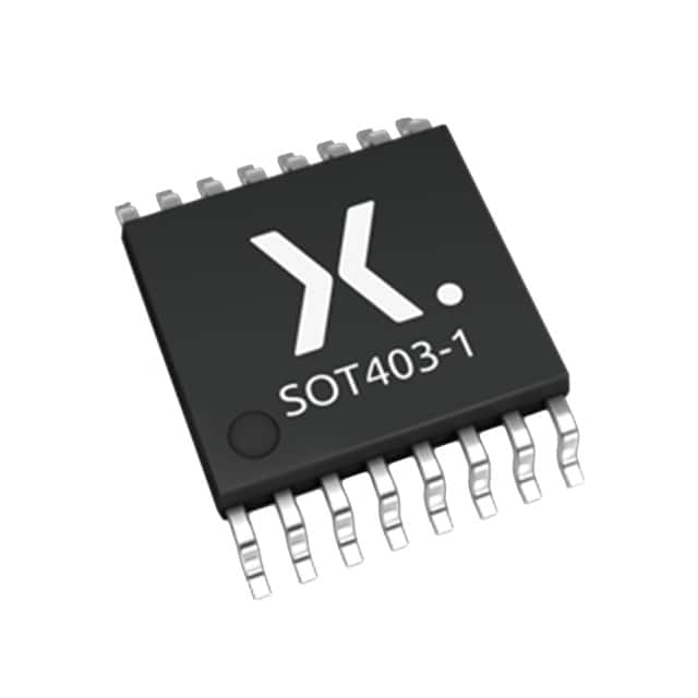
TSSOP16 plastic thin shrink small outline package (SOT403-1); 16 leads; body width 4.4 mm; 0.65 mm pitch; exposed pad not electrically connected.
| Pin/Terminal | Circuit Role | Design Meaning |
|---|---|---|
| 1 (PL) | Asynchronous parallel load input | Active-LOW signal that immediately captures D0–D7 into register stages, independent of clock - used for snapshot acquisition. |
| 2 (CP) | Clock input | LOW-to-HIGH edge-triggered; advances shift register only when CE = LOW - defines serial bit rate and synchronizes data movement. |
| 7 (Q7) | Serial output (MSB) | Provides the most significant bit of the 8-bit shift register after each CP edge - connects directly to MCU MISO or UART RX. |
| 9 (Q7) | Complementary serial output | Logical inverse of Q7 - enables differential signaling or noise-immune sampling in EMI-prone environments. |
| 10 (DS) | Serial data input | Accepts new bit during serial shift mode (PL = HIGH); sampled on CP rising edge when CE = LOW - feeds next stage during right-shift. |
| 11–14, 3–6 (D0–D7) | Parallel data inputs | Eight independent inputs accepting simultaneous 8-bit word; latched on PL falling edge - used for GPIO expansion or sensor bus readback. |
| 15 (CE) | Clock enable input | Active-LOW gate for CP - when HIGH, CP edges are ignored, freezing register state without requiring clock gating logic. |
| 16 (VCC) | Positive supply | Primary power rail; decoupling capacitor required within 5 mm to maintain switching noise immunity and timing integrity. |
| 8 (GND) | Ground reference | Signal and power return path; must be low-impedance plane to minimize ground bounce during parallel load transitions. |
Key Features
| Feature | Design Value |
|---|---|
| Asynchronous parallel load | Enables zero-latency capture of 8-bit status registers (e.g., switch banks or ADC result latches) without waiting for clock alignment. |
| TTL-compatible inputs | Eliminates need for external level translators when interfacing with 5 V sensors, encoders, or legacy controllers feeding 3.3 V MCUs. |
| Overvoltage tolerant inputs (15 V) | Permits direct connection to unregulated 12 V automotive lines or industrial 24 V I/O modules with internal clamping protection. |
| Complementary Q7/Q7 outputs | Supports balanced sampling or differential receiver interfaces, improving noise rejection in motor drive or CAN subsystem monitoring. |
| –40 °C to +125 °C operation | Validated for continuous use in engine control units, power inverters, and outdoor telecom equipment without thermal throttling. |
Applications
| Industrial PLC I/O Expansion | Automotive Body Control Module |
|---|---|
|
Use Scenario: Adding 8-channel digital input capability to a space-constrained PLC CPU board using existing 3-wire SPI interface. IC Role / Device Role / Timing Role: Parallel capture of pushbutton/limit switch states via PL, then serial streaming to MCU over CP/DS/Q7 at 5 MHz. Use Value: Reduces GPIO count requirement by 8 pins while maintaining deterministic 100 ns worst-case sampling-to-transfer latency. |
Use Scenario: Monitoring door lock status, window position, and mirror controls in a centralized BCM with limited MCU pin availability. IC Role / Device Role / Timing Role: Asynchronous latch of mechanical switch states on vehicle power-up (PL pulse), followed by periodic serial polling. Use Value: Enables single-wire serial diagnostics and eliminates 8 dedicated MCU input traces, reducing PCB layer count and BOM cost. |
| Embedded Data Acquisition Front-End | Legacy Equipment Interface Adapter |
|
Use Scenario: Digitizing analog sensor outputs from an 8-channel ADC with parallel output bus, feeding results to a low-pin-count ARM Cortex-M0+. IC Role / Device Role / Timing Role: Captures full 8-bit conversion result on ADC's BUSY deassertion (PL), then shifts out LSB-first via DS/Q7. Use Value: Achieves 100 kSPS effective throughput using only three MCU pins, avoiding resource-intensive parallel bus arbitration. |
Use Scenario: Interfacing vintage 8-bit parallel printer port signals (STROBE, ACK, BUSY) to modern USB-to-parallel adapters with microcontroller bridges. IC Role / Device Role / Timing Role: Latches parallel handshake signals on STROBE edge (PL), then serially reports status to bridge MCU for USB packet generation. Use Value: Preserves exact timing relationships between legacy control signals and USB transaction scheduling, preventing protocol timeouts. |
Equivalent & Alternatives
The following parts are listed as comparable options for similar 8-bit parallel-in/serial-out shift register applications.
| Alternative Part | Technical Difference | Application Difference | Selection Advice |
|---|---|---|---|
| 74HC165PW,112 | CMOS-input version; VIH min = 3.15 V @ VCC = 4.5 V; higher noise margin but requires ≥3.15 V logic high. | Better suited for mixed-voltage systems where all upstream drivers meet HC thresholds; less tolerant of marginal 3.3 V logic highs. | Select when interfacing exclusively with 5 V CMOS sources or when maximizing noise immunity is critical. |
| SN74LV165APWR | TI 3.3 V optimized; operates 2.0–5.5 V; VIH min = 1.7 V @ VCC = 3.3 V; lower propagation delay (10 ns typ). | Preferred for 3.3 V native systems; lacks 15 V overvoltage tolerance and extended temperature rating (–40 °C to +105 °C only). | Choose for high-speed, low-voltage embedded designs where industrial temp range is not required and overvoltage protection is handled externally. |
Compared with 74HC165PW,112 and SN74LV165APWR, the 74HCT165PW,112 uniquely balances TTL-level compatibility, 125 °C operation, and 15 V input tolerance - making it the only option among the three qualified for under-hood automotive and harsh industrial deployments with legacy 5 V signal sources.
Availability
74HCT165PW,112 is available at Aetrix Electronics and suitable for industrial PLC I/O expansion, automotive body control modules, embedded data acquisition front-ends, and legacy equipment interface adapters requiring stable component supply across extended temperature ranges.
Supply support for 74HCT165PW,112 includes scheduled delivery planning, volume procurement assistance, BOM continuity management, traceable sourcing, and lifecycle availability coordination for OEM customers, industrial embedded developers, connected-device designers, and electronics production programs.
Manufacturer
Nexperia is a global semiconductor expert delivering high-performance, reliable discrete, logic, and MOSFET devices with focus on efficiency, reliability, and sustainability.
The 74HCT165 forms part of Nexperia's industry-standard 74-series logic portfolio, engineered for robust interoperability in industrial automation, automotive electronics, and infrastructure systems demanding long-term supply stability and AEC-Q100-aligned qualification.
FAQ
What is the maximum clock frequency supported by the 74HCT165PW,112?
The 74HCT165PW,112 supports up to 26 MHz maximum clock frequency at VCC = 4.5 V and –40 °C to +85 °C ambient, and 17 MHz at full –40 °C to +125 °C range. These values are measured with CL = 50 pF and reflect guaranteed timing margins per Nexperia's Rev. 8 datasheet, Table 7.
Can the 74HCT165PW,112 operate with a 3.3 V supply?
No - the 74HCT165PW,112 is specified only for 4.5 V to 5.5 V operation per Table 5. At 3.3 V, input thresholds (VIH ≥ 2.0 V) may be met, but VOH/VOL, propagation delay, and temperature range are not guaranteed, and static current (ICC) may exceed limits due to incomplete transistor turn-on.
Is the exposed pad on the TSSOP16 package electrically connected?
No - the exposed thermal pad on SOT403-1 (TSSOP16) is not electrically connected to any internal node. Per datasheet Section 6.1 and Figure 12, it may remain floating or be connected to GND for thermal improvement, but no electrical function is assigned to it.
How does the CE (clock enable) input affect timing behavior?
When CE is HIGH, CP transitions are ignored - the register holds its state regardless of clock activity. This eliminates metastability risk during clock domain crossing and avoids unintended shifts during system reset or debug halts, unlike simple clock gating which may induce duty-cycle distortion.
74HCT165PW,112 Specifications
- Product attributes
- Attribute value
- Manufacturer:
- Nexperia USA Inc.
- Series:
- 74HCT
- Package/Case:
- 16-TSSOP (0.173", 4.40mm Width)
- Packaging:
- Tube
- Product Status:
- Obsolete
- Logic Type:
- Shift Register
- Output Type:
- Complementary
- Number of Elements:
- 1
- Number of Bits per Element:
- 8
- Function:
- Parallel or Serial to Serial
- Voltage - Supply:
- 4.5V ~ 5.5V
- Operating Temperature:
- -40°C ~ 125°C
- Grade:
- -
- Qualification:
- -
- Mounting Type:
- Surface Mount
- Supplier Device Package:
- 16-TSSOP
74HCT165PW,112 FAQ
1.How can I place an order for 74HCT165PW,112 through Aetrix?
Please submit a Request for Quotation (RFQ) for 74HCT165PW,112 on Aetrix. Our sales agent will provide a competitive quotation and guide you through the order confirmation once you accept the terms.
2.Are the price and stock information for 74HCT165PW,112 reliable?
The price and inventory of 74HCT165PW,112 are updated periodically and may fluctuate due to market conditions. Stock and pricing data are typically refreshed every 24 hours. Quotation validity for 74HCT165PW,112 is usually 5 days.
3.What payment methods are accepted for 74HCT165PW,112?
We accept Wire Transfer, PayPal, Credit Card, Western Union, MoneyGram, and Escrow for 74HCT165PW,112 transactions.
Note: Certain payment methods may incur a processing fee.
4.How is shipping managed for 74HCT165PW,112?
74HCT165PW,112 orders can be shipped via leading logistics carriers, including DHL, UPS, FedEx, TNT, or Registered Mail.
Once your 74HCT165PW,112 order is processed, you will receive an email with the shipment details and tracking number.
Note: Tracking information may take up to 24 hours to appear. Express delivery typically takes 3–5 business days.
5.How can I obtain technical support or documentation for 74HCT165PW,112?
For technical support, including 74HCT165PW,112 datasheets, pinout diagrams, or application guidance, please contact our engineering support team. They can provide detailed documentation and assistance for your 74HCT165PW,112 requirements.
6.How does Aetrix verify that 74HCT165PW,112 is sourced from the original manufacturer or authorized distributors?
All 74HCT165PW,112 products on Aetrix are procured from qualified distributors and authorized channels. Our dedicated quality assurance team conducts strict verification, including traceability checks and, if necessary, third-party testing. This ensures that 74HCT165PW,112 meets industry standards.
7.What is the process for return or replacement of 74HCT165PW,112?
All 74HCT165PW,112 units undergo pre-shipment inspection (PSI). If there is an issue with 74HCT165PW,112, returns or replacements are accepted under the following conditions:
1.Quantity discrepancies, incorrect items, or visible external defects (such as breakage or corrosion), acknowledged by Aetrix.
2.The issue is reported within 90 days of delivery.
3.The 74HCT165PW,112 part is unused and in its original packaging.
Return procedure for 74HCT165PW,112:
1.Submit a request within 90 days.
2.Obtain a Return Material Authorization (RMA) from Aetrix.
74HCT165PW,112 Tags

-
SN74HC164DR
Texas Instruments

-
SN74HC595DR
Texas Instruments
-
74HC595PW,118
Nexperia USA Inc.

-
SN74HC165PWR
Texas Instruments
-
HEF4094BT,653
Nexperia USA Inc.
-
74HC595D,118
Nexperia USA Inc.
-
SN74HC595PWR
Texas Instruments
-
74HC165D,653
Nexperia USA Inc.
-
SN74LV165APWR
Texas Instruments
-
74HC595BQ,115
Nexperia USA Inc.
-
74HC165BQ,115
Nexperia USA Inc.
-
CD4094BPWR
Texas Instruments
Tech Hub

An engineering guide to LED driver operation, constant-current and constant-voltage outputs, linear and switching topologies, dimming, IC selection, calculations, replacement compatibility, and fault c…

Operational amplifier guide covering op amp basics, feedback, ideal vs real op amps, common configurations, buffer circuits, offset, bias current, gain-bandwidth, slew rate, rail-to-rail limits and sel…

Jumper cables guide covering safe connection order, red and black clamp placement, final ground connection, cable gauge, length, clamp quality, copper vs CCA cables, jump starter comparison and battery…

LDO regulator guide covering low dropout voltage, power dissipation, thermal design, PSRR, output noise, capacitor stability, adjustable LDO circuits, LDO vs buck converter and datasheet selection chec…

Conditional Access Module guide covering CAM meaning, CI/CI+ interface, smart card authorization, DVB security workflow, TV and set-top box compatibility, internal electronics, ESD protection, connecto…

Guide to electronic component obsolescence covering EOL risk, PCN/PDN notices, last-time buy planning, replacement options, form-fit-function validation, counterfeit risk and BOM lifecycle management.

18650 battery guide covering lithium-ion cell basics, 3.6V/3.7V voltage, 4.2V charging, mAh and Wh capacity, protected cells, chargers, BMS, series-parallel packs, holders, welding and sourcing checks.…

Hall effect sensor guide covering working principle, linear and digital sensors, Arduino circuits, current sensing, speed detection, automotive applications, A3144 examples, signal filtering and datash…

Product Change Notification guide for electronic components, covering PCN meaning, PCN vs PDN/EOL, common change types, risk levels, form-fit-function review, engineering validation, BOM control, LTB/L…

A practical guide to blend door actuators, covering HVAC function, symptoms, location, AC and heater issues, reset and calibration, replacement cost, electrical diagnosis, compatibility checks, and rep…


