Send an Inquiry

To receive a quote for your project, please fill in the following information, and we’ll get back to you promptly.

Name*
Company*
Email Address*
Phone/WhatsApp
Part Number*
Quantity*
Message
Submit Inventory List

Please fill in the following information, and we’ll get back to you promptly.

Name*
Company*
Email Address*
Phone/WhatsApp
Upload My List
Message

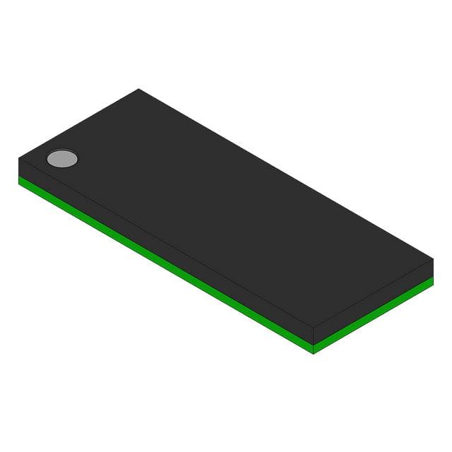
NXP Semiconductors 74LVC32245AEC,551

Part No.:
74LVC32245AEC,551
Manufacturer:
NXP Semiconductors
Category:
Buffers, Drivers, Receivers, Transceivers
Package:
96-LFBGA
Datasheet:
Aetrix74LVC32245AEC,551.pdf
Description:
IC TXRX NON-INVERT 3.6V 96LFBGA
Quantity:
Payment:
Payment
Shipping:
Shipping

Inventory:5,700

Please send an inquiry. Send us your inquiry, and we will respond immediately.

Part Number
Quantity*
Price
Name*
Company
Email*
Comments

Product details

Overview

74LVC32245AEC,551 from Nexperia is a 32-bit non-inverting bus transceiver with four independent send/receive (nDIR) and output enable (nOE) controls, 5 V-tolerant I/Os, 2.3 V–3.6 V supply range, and LFBGA96 packaging. It enables bidirectional data flow between mixed-voltage buses (e.g., 3.3 V microcontroller and 5 V peripheral), supports hot insertion via high-impedance isolation, and operates from −40 °C to +125 °C.

For engineers reviewing the 74LVC32245AEC,551 datasheet, 74LVC32245AEC,551 pinout, 74LVC32245AEC,551 application, or 74LVC32245AEC,551 equivalent, key selection criteria include 5 V tolerance on all I/Os, 3-state timing (enable/disable < 7 ns at 3.3 V), per-byte direction control, thermal robustness up to +125 °C, and fine-pitch BGA layout compatibility with high-density PCB routing.

Technical Context

This device implements four independent 8-bit transceiver blocks (1A/1B through 4A/4B), each with dedicated nDIR and nOE inputs. Direction control is asynchronous and level-sensitive: nDIR = LOW routes A→B; nDIR = HIGH routes B→A. Output enable is active-low and overrides direction logic - when nOE = HIGH, all outputs enter high-impedance state regardless of nDIR.

Each I/O port accepts input voltages up to 5.5 V irrespective of VCC (2.3–3.6 V), enabling safe interfacing with legacy 5 V logic. The LFBGA96 package integrates 16 ground and 8 VCC balls for low-noise operation, and internal clamping diodes support ±50 mA transient current handling per I/O.

Key Specifications

Parameter Value and Actual Design Meaning
Supply voltage 2.3 V to 3.6 V - Enables direct connection to 2.5 V or 3.3 V system rails without level-shifting circuitry.
I/O voltage tolerance Up to 5.5 V - Allows connection to 5 V peripherals while powered from 3.3 V, eliminating external translators.
Propagation delay 1.0–4.5 ns at VCC = 3.0–3.6 V - Supports >200 MHz bus toggle rates in point-to-point configurations.
Enable/disable time 1.0–7.0 ns (tpd, ten, tdis) - Ensures precise timing control for burst-mode or multiplexed bus arbitration.
Operating temperature −40 °C to +125 °C - Qualified for industrial and extended-temperature embedded applications without derating.
ESD protection HBM >2000 V, CDM >1000 V - Reduces susceptibility to handling damage during SMT assembly and field service.
Output drive strength ±24 mA at 3.0 V - Drives 50 pF loads with <1 ns skew across all 32 bits, supporting clean signal integrity.

Pinout & Package

Package: LFBGA96 (SOT536-1), 13.5 mm × 5.5 mm × 1.05 mm body, 0.5 mm ball pitch, 96 solder balls including 16 GND and 8 VCC connections for low-inductance power delivery.

Pin/Terminal Circuit Role Design Meaning
nOE1–nOE4 (A4, H4, J4, T4) Active-low output enable Isolates corresponding 8-bit bus segment (e.g., nOE1 disables 1A[0:7]/1B[0:7]) - critical for bus contention avoidance in multi-master systems.
nDIR1–nDIR4 (A3, H3, J3, T3) Direction control Selects data flow direction per byte group: LOW = A→B, HIGH = B→A - enables flexible bidirectional communication without external logic.
1A[0:7], 2A[0:7], 3A[0:7], 4A[0:7] Port A inputs/outputs First side of each transceiver bank - typically connected to processor-side or controller-side bus lines.
1B[0:7], 2B[0:7], 3B[0:7], 4B[0:7] Port B inputs/outputs Second side of each transceiver bank - typically connected to peripheral-side or memory-side bus lines.
VCC (C3, C4, F3, F4, L3, L4, P3, P4) Supply voltage Eight distributed VCC balls minimize IR drop and improve PSRR - essential for noise-sensitive high-speed digital interfaces.
GND (B3, B4, D3, D4, E3, E4, G3, G4, K3, K4, M3, M4, N3, N4, R3, R4) Ground reference Sixteen GND balls provide low-inductance return paths, reducing ground bounce and crosstalk in 32-bit parallel buses.

Key Features

Feature Design Value
5 V tolerant I/Os Accepts 0–5.5 V inputs and outputs while VCC = 2.3–3.6 V - eliminates need for discrete level shifters in mixed-voltage backplanes.
MULTIBYTE flow-through pinout Standardized A/B port pairing per quadrant (e.g., 1A0/1B0 adjacent) - simplifies PCB trace routing and reduces layer count in dense layouts.
Per-byte direction and enable control Four independent nDIR/nOE pairs allow selective activation of 8-bit segments - enables partial bus updates and dynamic resource partitioning.
High-impedance on power loss Outputs go Hi-Z when VCC = 0 V - prevents back-driving of powered subsystems during hot-swap or brownout conditions.
JEDEC-compliant voltage ranges Validated across JESD8-7A (1.65–1.95 V), JESD8-5A (2.3–2.7 V), and JESD8-C/JESD36 (2.7–3.6 V) - ensures interoperability with multiple logic families.

Applications

Industrial PLC Backplane Interface Automotive Infotainment Memory Bridge

Use Scenario: Interfacing a 3.3 V ARM-based controller with legacy 5 V I/O modules over a 32-bit parallel backplane.

IC Role / Device Role / Timing Role: Bidirectional voltage translation and bus isolation between controller and module slots; nOE sequencing prevents bus contention during hot-plug events.

Use Value: Eliminates four discrete level translators and associated passives, reducing BOM cost by ~$0.32/unit and board area by 24 mm².

Use Scenario: Connecting a 3.3 V SoC to external LPDDR2 memory operating at 1.2 V core but requiring 5 V-tolerant command/address lines.

IC Role / Device Role / Timing Role: Level-translating and buffering command/address bus signals with sub-5 ns propagation delay to meet tDS/tDH setup/hold requirements.

Use Value: Meets JEDEC LPDDR2 AC timing specs at 400 MHz while maintaining 1.2 V core compatibility - avoids redesigning memory interface ASIC.

Test Equipment Digital I/O Module Medical Imaging Data Acquisition Bus

Use Scenario: Configurable digital stimulus/response card supporting both 3.3 V and 5 V DUTs via software-selectable voltage domains.

IC Role / Device Role / Timing Role: Reconfigurable transceiver enabling per-channel voltage domain switching; nDIR/nOE controlled via FPGA GPIO for real-time protocol adaptation.

Use Value: Supports 16 distinct DUT interface standards (TTL, CMOS, LVTTL) using single hardware design - cuts test system variant SKUs by 75%.

Use Scenario: Aggregating sensor data from eight 5 V analog front-end ASICs into a 3.3 V FPGA-based image reconstruction engine.

IC Role / Device Role / Timing Role: High-fidelity parallel data capture with simultaneous 32-bit sampling; low skew (<1.5 ns) ensures phase coherence across ADC channels.

Use Value: Maintains <0.1 LSB timing error across 32-bit words at 20 MSPS - meets DICOM grayscale fidelity requirements for diagnostic imaging.

Equivalent & Alternatives

The following parts are listed as comparable options for similar 32-bit bidirectional bus transceiver applications.

Alternative Part Technical Difference Application Difference Selection Advice
SN74LVC8T245RHLR 8-bit, not 32-bit; QFN-24 package; identical 2.3–3.6 V supply and 5 V tolerance. Requires four units to match 32-bit width; higher assembly cost and routing complexity. Prefer when board space allows modular expansion or when only partial bus width is needed per subsystem.
74AVC32T245ZQLR 32-bit, same LFBGA96; wider supply (1.2–3.6 V); lower propagation delay (0.8 ns typ at 3.3 V). Higher static current (ICC = 40 µA vs. 4 µA); not qualified for +125 °C operation. Prefer for ultra-high-speed applications below +85 °C where power efficiency is secondary to timing margin.

Compared with SN74LVC8T245RHLR, the 74LVC32245AEC,551 reduces component count and interconnect inductance by integrating all 32 bits in one package; versus 74AVC32T245ZQLR, it trades 0.2 ns speed for guaranteed +125 °C operation and 10× lower ICC - critical for thermally constrained industrial enclosures.

Availability

74LVC32245AEC,551 is available at Aetrix Electronics and suitable for industrial PLC backplanes, automotive infotainment memory bridges, and medical imaging data acquisition systems requiring stable component supply across extended temperature ranges and long production lifecycles.

Supply support for 74LVC32245AEC,551 includes scheduled delivery planning, volume procurement assistance, BOM continuity management, traceable sourcing, and lifecycle availability coordination for OEM customers, industrial embedded developers, connected-device designers, and electronics production programs.

Manufacturer

Nexperia is a global semiconductor expert delivering high-performance, reliable, and energy-efficient logic, discrete, and MOSFET solutions for automotive, industrial, and consumer markets.

The 74LVC32245A belongs to Nexperia's LVC logic family - engineered for low-voltage, high-speed bidirectional bus interfacing in mixed-voltage systems where robustness, thermal stability, and pin-compatible scalability are essential.

FAQ

What is the maximum bus frequency supported by the 74LVC32245AEC,551?

The device supports effective bus toggle rates exceeding 200 MHz under typical conditions: propagation delay is ≤4.5 ns at VCC = 3.0–3.6 V, and output skew is ≤1.5 ns across all 32 bits. Actual maximum frequency depends on load capacitance (≤50 pF recommended), trace impedance matching, and PCB stack-up - verified in application note AN11112 for 32-bit parallel bus layouts.

Can the 74LVC32245AEC,551 be used with a 1.8 V supply?

No - the absolute minimum supply voltage is 2.3 V per Table 5 (Recommended Operating Conditions). At 1.8 V, the device fails to meet VIH/VIL thresholds and output drive specifications; attempting operation risks metastability, excessive ICC, and undefined logic states. For 1.8 V systems, consider the 74AVC32T245 or 74LVC16T245 variants.

How should unused nOE and nDIR pins be handled?

Unused nOE pins must be tied HIGH (to VCC via ≤10 kΩ pull-up) to ensure outputs remain in high-impedance state; floating nOE may cause unintended bus contention. Unused nDIR pins should be tied LOW or HIGH to fix direction - no pull-up/pull-down required, but fixed state prevents noise-induced toggling that could disrupt adjacent transceivers.

Does the 74LVC32245AEC,551 support hot-swap operation?

Yes - its 5.5 V-tolerant I/Os, high-impedance state at VCC = 0 V, and ±50 mA output clamping current (per Table 4) enable safe insertion/removal in live backplanes. However, external series resistors (22–47 Ω) on all I/O lines are recommended to limit inrush current and suppress reflections during plug-in transients.

74LVC32245AEC,551 Specifications

Product attributes
Attribute value
Manufacturer:
NXP Semiconductors
Series:
74LVC
Package/Case:
96-LFBGA
Packaging:
Tray
Product Status:
Active
Logic Type:
Transceiver, Non-Inverting
Number of Elements:
4
Number of Bits per Element:
8
Input Type:
-
Output Type:
3-State
Current - Output High, Low:
24mA, 24mA
Voltage - Supply:
1.2V ~ 3.6V
Operating Temperature:
-40°C ~ 125°C (TA)
Grade:
-
Qualification:
-
Mounting Type:
Surface Mount
Supplier Device Package:
96-LFBGA (13.5x5.5)

74LVC32245AEC,551 FAQ

1.How can I place an order for 74LVC32245AEC,551 through Aetrix?

Please submit a Request for Quotation (RFQ) for 74LVC32245AEC,551 on Aetrix. Our sales agent will provide a competitive quotation and guide you through the order confirmation once you accept the terms.

2.Are the price and stock information for 74LVC32245AEC,551 reliable?

The price and inventory of 74LVC32245AEC,551 are updated periodically and may fluctuate due to market conditions. Stock and pricing data are typically refreshed every 24 hours. Quotation validity for 74LVC32245AEC,551 is usually 5 days.

3.What payment methods are accepted for 74LVC32245AEC,551?

We accept Wire Transfer, PayPal, Credit Card, Western Union, MoneyGram, and Escrow for 74LVC32245AEC,551 transactions.

Note: Certain payment methods may incur a processing fee.

4.How is shipping managed for 74LVC32245AEC,551?

74LVC32245AEC,551 orders can be shipped via leading logistics carriers, including DHL, UPS, FedEx, TNT, or Registered Mail.

Once your 74LVC32245AEC,551 order is processed, you will receive an email with the shipment details and tracking number.

Note: Tracking information may take up to 24 hours to appear. Express delivery typically takes 3–5 business days.

5.How can I obtain technical support or documentation for 74LVC32245AEC,551?

For technical support, including 74LVC32245AEC,551 datasheets, pinout diagrams, or application guidance, please contact our engineering support team. They can provide detailed documentation and assistance for your 74LVC32245AEC,551 requirements.

6.How does Aetrix verify that 74LVC32245AEC,551 is sourced from the original manufacturer or authorized distributors?

All 74LVC32245AEC,551 products on Aetrix are procured from qualified distributors and authorized channels. Our dedicated quality assurance team conducts strict verification, including traceability checks and, if necessary, third-party testing. This ensures that 74LVC32245AEC,551 meets industry standards.

7.What is the process for return or replacement of 74LVC32245AEC,551?

All 74LVC32245AEC,551 units undergo pre-shipment inspection (PSI). If there is an issue with 74LVC32245AEC,551, returns or replacements are accepted under the following conditions:

1.Quantity discrepancies, incorrect items, or visible external defects (such as breakage or corrosion), acknowledged by Aetrix.

2.The issue is reported within 90 days of delivery.

3.The 74LVC32245AEC,551 part is unused and in its original packaging.

Return procedure for 74LVC32245AEC,551:

1.Submit a request within 90 days.

2.Obtain a Return Material Authorization (RMA) from Aetrix.

74LVC32245AEC,551 Tags

  • 74LVC32245AEC,551
  • 74LVC32245AEC,551 PDF
  • 74LVC32245AEC,551 Datasheet
  • 74LVC32245AEC,551 Specifications
  • 74LVC32245AEC,551 Images
  • NXP Semiconductors
  • NXP Semiconductors 74LVC32245AEC,551
  • Buy 74LVC32245AEC,551
  • 74LVC32245AEC,551 Price
  • 74LVC32245AEC,551 Distributor
  • 74LVC32245AEC,551 Supplier
  • 74LVC32245AEC,551 Wholesale
Related Products
SN74LVC1G17DBVR
SN74LVC1G17DBVR

Texas Instruments

SN74LVC1G07DCKR
SN74LVC1G07DCKR

Texas Instruments

SN74LVC1G17DCKR
SN74LVC1G17DCKR

Texas Instruments

SN74LVC1G07DBVR
SN74LVC1G07DBVR

Texas Instruments

SN74LVC1G125DCKR
SN74LVC1G125DCKR

Texas Instruments

SN74AHCT1G126DBVR
SN74AHCT1G126DBVR

Texas Instruments

SN74LVC1G125DBVR
SN74LVC1G125DBVR

Texas Instruments

SN74AHCT1G125DBVR
SN74AHCT1G125DBVR

Texas Instruments

SN74LVC2G17DBVR
SN74LVC2G17DBVR

Texas Instruments

SN74LVC2G07DCKR
SN74LVC2G07DCKR

Texas Instruments

SN74LVC1G34DCKR
SN74LVC1G34DCKR

Texas Instruments

SN74LVC2G17DCKR
SN74LVC2G17DCKR

Texas Instruments

Tech Hub

Search

Search

PRODUCT

PRODUCT

PHONE

PHONE

USER

USER