
 My Inquiry
 My Account


Nexperia USA Inc. 74LVC823ADB,112
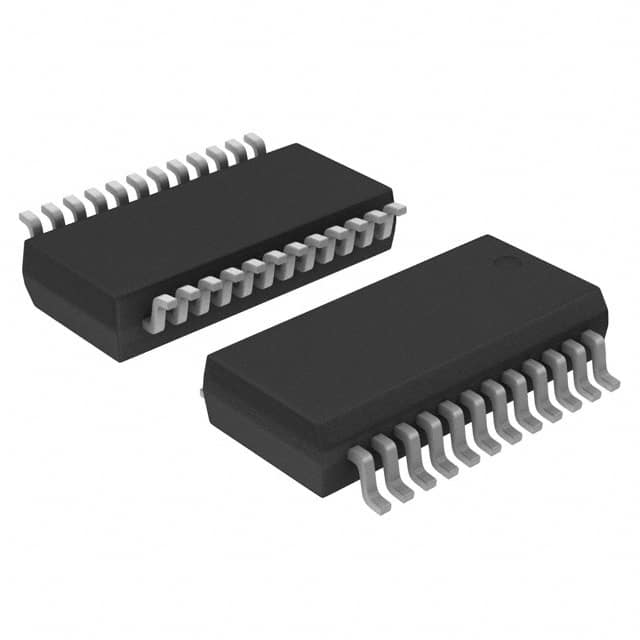
- Part No.:
- 74LVC823ADB,112
- Manufacturer:
- Nexperia USA Inc.
- Category:
- Flip Flops
- Package:
- 24-SSOP (0.209", 5.30mm Width)
- Datasheet:
-
 74LVC823ADB,112.pdf
- Description:
- IC FF D-TYPE SNGL 9BIT 24SSOP
- Quantity:
- Payment:

- Shipping:

Inventory:3,665
Please send an inquiry. Send us your inquiry, and we will respond immediately.
Product details
Overview
74LVC823ADB,112 from Nexperia is a 9-bit positive-edge-triggered D-type flip-flop with independent clock enable (CE), master reset (MR), and 3-state outputs (Q0–Q8), operating from 1.2 V to 3.6 V supply. It features 5 V tolerant inputs/outputs, enabling mixed-voltage bus interfacing between 3.3 V logic and legacy 5 V systems. Its flow-through pinout supports clean PCB routing in data-path applications such as industrial I/O expansion and memory address latching.
For engineers reviewing the 74LVC823ADB,112 datasheet, 74LVC823ADB,112 pinout, 74LVC823ADB,112 application, or 74LVC823ADB,112 equivalent, key selection criteria include 5 V tolerance on all I/Os, guaranteed operation up to +125 °C, tpd ≤ 8.0 ns at 3.3 V, fmax ≥ 150 MHz, and SO24 package compatibility with JEDEC SOT137-1 footprint.
Technical Context
This device implements nine synchronous D-flip-flops sharing a common clock (CP) input and individually controllable via CE and MR. The 3-state output buffer is decoupled from register operation - OE controls output impedance without affecting stored state. All inputs meet TTL voltage thresholds across the full 1.2 V–3.6 V VCC range.
Internal logic ensures setup/hold times are met for Dn and CE relative to CP's rising edge, with tsu = 1.3 ns and th = 1.3 ns at VCC = 3.3 V. Output skew is tightly controlled at ≤1.0 ns (typ), critical for parallel data capture integrity in high-speed digital interfaces.
Key Specifications
| Parameter | Value and Actual Design Meaning |
|---|---|
| Logic Function | 9-bit positive-edge-triggered D-type flip-flop with 3-state outputs |
| Supply Voltage Range | 1.2 V to 3.6 V - enables direct interface with 1.8 V, 2.5 V, and 3.3 V systems |
| I/O Voltage Tolerance | Up to 5.5 V - allows safe connection to 5 V buses without level shifters |
| Propagation Delay (tpd) | ≤ 8.0 ns at VCC = 3.3 V - supports >120 MHz system clock rates |
| Maximum Frequency (fmax) | 150 MHz at VCC = 3.0–3.6 V - suitable for high-speed data latching |
| Operating Temperature | −40 °C to +125 °C - qualified for automotive under-hood and industrial control environments |
| Output Skew (tsk(o)) | ≤ 1.0 ns - ensures simultaneous valid data across all 9 outputs |
Pinout & Package
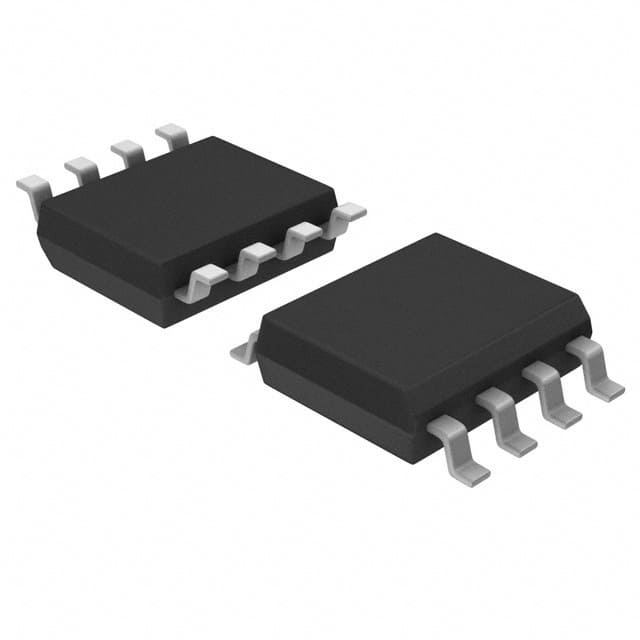
74LVC823ADB,112 is supplied in SO24 plastic small outline package (SOT137-1), 24-pin, 7.5 mm body width, with standard gull-wing leads and pin 1 index marker.
| Pin/Terminal | Circuit Role | Design Meaning |
|---|---|---|
| 1 | OE | Active-low 3-state output enable - disables Q0–Q8 simultaneously without altering register contents |
| 2–10 | D0–D8 | Data inputs - sampled on rising CP edge when CE = LOW |
| 11 | MR | Active-low master reset - forces all Qn to LOW regardless of CP or CE state |
| 12 | GND | Ground reference - 0 V return path for all internal logic and I/O |
| 13 | CP | Clock input - rising-edge trigger for synchronous data capture |
| 14 | CE | Active-low clock enable - blocks CP from updating registers when HIGH |
| 15–23 | Q0–Q8 | 3-state outputs - reflect Dn state when OE = LOW; high-Z when OE = HIGH |
| 24 | VCC | Power supply - supplies core logic and I/O buffers; must be decoupled locally |
Key Features
| Feature | Design Value |
|---|---|
| 5 V tolerant I/O | Enables direct interconnection with 5 V peripherals while powered from 3.3 V or lower rails |
| Independent register & output control | MR and CE affect only flip-flop state; OE affects only output drivers - no functional coupling |
| Flow-through pinout | Input-to-output signal path runs left-to-right across package - minimizes trace crossovers on PCB |
| Wide temperature range | Specified from −40 °C to +125 °C - meets AEC-Q100 Grade 1 requirements for automotive use |
| Low dynamic power | CPD = 16.4 pF at VCC = 3.3 V - enables low-power operation in battery-backed or thermally constrained systems |
Applications
| Industrial PLC I/O Expansion | Automotive Body Control Module |
|---|---|
Use Scenario: Latching sensor status signals (e.g., door open/closed, seatbelt buckle) before multiplexed transmission to MCU. IC Role / Device Role / Timing Role: 9-bit parallel data register synchronizing asynchronous mechanical switch inputs to a deterministic clock domain. Use Value: Eliminates metastability risk with 1.3 ns setup/hold margin at 3.3 V and provides 5 V tolerance for direct connection to 5 V pull-up sensors. | Use Scenario: Buffering and isolating CAN transceiver TX/RX lines and discrete actuator control signals in centralized body electronics units. IC Role / Device Role / Timing Role: Level-translating latch for bidirectional signal conditioning between 3.3 V microcontroller GPIO and 5 V legacy subsystems. Use Value: Enables single-supply 3.3 V MCU design while maintaining interoperability with existing 5 V lighting, HVAC, and mirror control modules. |
| Memory Address Latching | Test Equipment Digital Pattern Generator |
Use Scenario: Capturing and holding upper address bits during multiplexed address/data bus cycles in FPGA-based memory controllers. IC Role / Device Role / Timing Role: High-speed 9-bit address register with precise timing alignment to system clock edges. Use Value: Achieves <8 ns propagation delay and <1 ns output skew - ensures setup time compliance for SRAM/Flash access at 100+ MHz. | Use Scenario: Generating synchronized parallel stimulus vectors for IC functional testing using pattern memory and clocked output staging. IC Role / Device Role / Timing Role: Deterministic 9-bit output staging register feeding into high-speed DAC or comparator arrays. Use Value: Guarantees simultaneous edge-aligned updates across all 9 outputs (≤1 ns skew), critical for coherent multi-channel waveform generation. |
Equivalent & Alternatives
The following parts are listed as comparable options for similar 9-bit D-type flip-flop applications.
| Alternative Part | Technical Difference | Application Difference | Selection Advice |
|---|---|---|---|
| 74LVC823APW,118 | TSSOP24 package (SOT355-1); 4.4 mm body width; 0.65 mm pitch | Higher board density; requires finer-pitch reflow profile; slightly higher thermal resistance | Select for space-constrained designs where SO24 footprint is unavailable |
| SN74LVC823APWR | TI-manufactured; identical logic function; same SO24 pinout; ±10% tpd variation at 3.3 V | No change in system-level behavior; validated for same industrial temp range | Use when dual-sourcing or TI-specific qualification is required |
Compared with 74LVC823ADB,112, the TSSOP variant reduces PCB area but increases assembly complexity, while the TI alternative offers second-source assurance without functional or timing trade-offs - both retain full 5 V I/O tolerance and −40 °C to +125 °C operation.
Availability
74LVC823ADB,112 is available at Aetrix Electronics and suitable for industrial PLC I/O expansion, automotive body control modules, memory address latching, and test equipment digital pattern generation requiring stable component supply across extended temperature ranges.
Supply support for 74LVC823ADB,112 includes scheduled delivery planning, volume procurement assistance, BOM continuity management, traceable sourcing, and lifecycle availability coordination for OEM customers, industrial embedded developers, connected-device designers, and electronics production programs.
Manufacturer
Nexperia is a global semiconductor expert delivering high-performance logic, analog, and MOSFET solutions optimized for efficiency, reliability, and miniaturization in high-volume applications.
The 74LVC series targets low-voltage, high-speed digital interfacing with 5 V tolerance - designed specifically for mixed-supply systems in industrial automation, automotive electronics, and communications infrastructure.
FAQ
What is the maximum clock frequency supported by 74LVC823ADB,112?
The 74LVC823ADB,112 supports a maximum clock frequency of 150 MHz at VCC = 3.0 V to 3.6 V and −40 °C to +125 °C ambient. At 3.3 V, typical fmax is 200 MHz, but the guaranteed minimum is 150 MHz per datasheet Table 7. This rating assumes proper signal integrity, load capacitance ≤50 pF, and clean power supply decoupling.
Can 74LVC823ADB,112 safely interface with 5 V microcontrollers?
Yes - all inputs and outputs are rated for 5.5 V absolute maximum and fully 5 V tolerant when VCC is 1.2 V to 3.6 V. Inputs accept 5 V logic levels directly, and outputs drive 5 V buses in high-Z or active states without damage or level-shifting circuitry, as confirmed in Section 1 and Table 4 of the datasheet.
How does the master reset (MR) interact with clock enable (CE)?
MR is asynchronous and dominant: a LOW on MR forces all Qn outputs to LOW immediately, overriding CE, CP, and Dn states. CE only gates CP's effect on register updates; it has no influence on MR's reset action. This behavior is explicitly defined in Table 3 (Function Table) and Figure 4 (Logic Diagram).
Is the SO24 package of 74LVC823ADB,112 RoHS-compliant and lead-free?
Yes - the 74LVC823ADB,112 in SO24 (SOT137-1) package is manufactured per RoHS Directive 2011/65/EU and is lead-free, halogen-free, and compliant with Nexperia's environmental specifications. Full compliance documentation, including substance declarations and test reports, is available upon request from Aetrix Electronics.
74LVC823ADB,112 Specifications
- Product attributes
- Attribute value
- Manufacturer:
- Nexperia USA Inc.
- Series:
- 74LVC
- Package/Case:
- 24-SSOP (0.209", 5.30mm Width)
- Packaging:
- Tube
- Product Status:
- Not For New Designs
- Function:
- Master Reset
- Type:
- D-Type
- Output Type:
- Tri-State, Non-Inverted
- Number of Elements:
- 1
- Number of Bits per Element:
- 9
- Clock Frequency:
- 200 MHz
- Max Propagation Delay @ V, Max CL:
- 10ns @ 3.3V, 50pF
- Trigger Type:
- Positive Edge
- Current - Output High, Low:
- 24mA, 24mA
- Voltage - Supply:
- 1.65V ~ 3.6V
- Current - Quiescent (Iq):
- 10 µA
- Input Capacitance:
- 5 pF
- Operating Temperature:
- -40°C ~ 125°C (TA)
- Grade:
- -
- Qualification:
- -
- Mounting Type:
- Surface Mount
- Supplier Device Package:
- 24-SSOP
74LVC823ADB,112 FAQ
1.How can I place an order for 74LVC823ADB,112 through Aetrix?
Please submit a Request for Quotation (RFQ) for 74LVC823ADB,112 on Aetrix. Our sales agent will provide a competitive quotation and guide you through the order confirmation once you accept the terms.
2.Are the price and stock information for 74LVC823ADB,112 reliable?
The price and inventory of 74LVC823ADB,112 are updated periodically and may fluctuate due to market conditions. Stock and pricing data are typically refreshed every 24 hours. Quotation validity for 74LVC823ADB,112 is usually 5 days.
3.What payment methods are accepted for 74LVC823ADB,112?
We accept Wire Transfer, PayPal, Credit Card, Western Union, MoneyGram, and Escrow for 74LVC823ADB,112 transactions.
Note: Certain payment methods may incur a processing fee.
4.How is shipping managed for 74LVC823ADB,112?
74LVC823ADB,112 orders can be shipped via leading logistics carriers, including DHL, UPS, FedEx, TNT, or Registered Mail.
Once your 74LVC823ADB,112 order is processed, you will receive an email with the shipment details and tracking number.
Note: Tracking information may take up to 24 hours to appear. Express delivery typically takes 3–5 business days.
5.How can I obtain technical support or documentation for 74LVC823ADB,112?
For technical support, including 74LVC823ADB,112 datasheets, pinout diagrams, or application guidance, please contact our engineering support team. They can provide detailed documentation and assistance for your 74LVC823ADB,112 requirements.
6.How does Aetrix verify that 74LVC823ADB,112 is sourced from the original manufacturer or authorized distributors?
All 74LVC823ADB,112 products on Aetrix are procured from qualified distributors and authorized channels. Our dedicated quality assurance team conducts strict verification, including traceability checks and, if necessary, third-party testing. This ensures that 74LVC823ADB,112 meets industry standards.
7.What is the process for return or replacement of 74LVC823ADB,112?
All 74LVC823ADB,112 units undergo pre-shipment inspection (PSI). If there is an issue with 74LVC823ADB,112, returns or replacements are accepted under the following conditions:
1.Quantity discrepancies, incorrect items, or visible external defects (such as breakage or corrosion), acknowledged by Aetrix.
2.The issue is reported within 90 days of delivery.
3.The 74LVC823ADB,112 part is unused and in its original packaging.
Return procedure for 74LVC823ADB,112:
1.Submit a request within 90 days.
2.Obtain a Return Material Authorization (RMA) from Aetrix.
74LVC823ADB,112 Tags

-
SN74HC74DR
Texas Instruments

-
SN74HC74PWR
Texas Instruments
-
74LVC1G74GT,115
Nexperia USA Inc.

-
SN74LVC2G74DCUR
Texas Instruments
-
CD4013BM96
Texas Instruments

-
SN74HCT273PWR
Texas Instruments
-
SN74LVC1G74DCUR
Texas Instruments
-
SN74HC574DWR
Texas Instruments
-
74LVC1G74DC,125
Nexperia USA Inc.
-
SN74HC273DWR
Texas Instruments
-
SN74HCT574DWR
Texas Instruments
-
SN74LVC1G74DCTR
Texas Instruments
Tech Hub

An engineering guide to LED driver operation, constant-current and constant-voltage outputs, linear and switching topologies, dimming, IC selection, calculations, replacement compatibility, and fault c…

Operational amplifier guide covering op amp basics, feedback, ideal vs real op amps, common configurations, buffer circuits, offset, bias current, gain-bandwidth, slew rate, rail-to-rail limits and sel…

Jumper cables guide covering safe connection order, red and black clamp placement, final ground connection, cable gauge, length, clamp quality, copper vs CCA cables, jump starter comparison and battery…

LDO regulator guide covering low dropout voltage, power dissipation, thermal design, PSRR, output noise, capacitor stability, adjustable LDO circuits, LDO vs buck converter and datasheet selection chec…

Conditional Access Module guide covering CAM meaning, CI/CI+ interface, smart card authorization, DVB security workflow, TV and set-top box compatibility, internal electronics, ESD protection, connecto…

Guide to electronic component obsolescence covering EOL risk, PCN/PDN notices, last-time buy planning, replacement options, form-fit-function validation, counterfeit risk and BOM lifecycle management.

18650 battery guide covering lithium-ion cell basics, 3.6V/3.7V voltage, 4.2V charging, mAh and Wh capacity, protected cells, chargers, BMS, series-parallel packs, holders, welding and sourcing checks.…

Hall effect sensor guide covering working principle, linear and digital sensors, Arduino circuits, current sensing, speed detection, automotive applications, A3144 examples, signal filtering and datash…

Product Change Notification guide for electronic components, covering PCN meaning, PCN vs PDN/EOL, common change types, risk levels, form-fit-function review, engineering validation, BOM control, LTB/L…

A practical guide to blend door actuators, covering HVAC function, symptoms, location, AC and heater issues, reset and calibration, replacement cost, electrical diagnosis, compatibility checks, and rep…


