
 My Inquiry
 My Account


Renesas 82P2816BBG
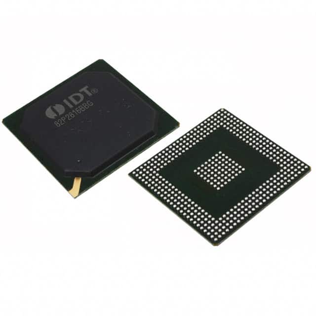
- Part No.:
- 82P2816BBG
- Manufacturer:
- Renesas
- Category:
- Telecom
- Package:
- 416-BGA
- Datasheet:
-
 82P2816BBG.pdf
- Description:
- IC TELECOM INTERFACE 416BGA
- Quantity:
- Payment:

- Shipping:

Inventory:4,810
Please send an inquiry. Send us your inquiry, and we will respond immediately.
Product details
Overview
82P2816BBG from Integrated Device Technology is a 16(+1) channel high-density T1/E1/J1 line interface unit (LIU) designed for carrier-grade telecom access equipment. It integrates full receive and transmit signal conditioning, jitter attenuation, PRBS pattern generation/detection, and dual-loopback diagnostics per channel. Key confirmed parameters include 16 data channels + 1 maintenance channel, support for T1 (1.544 Mbps), E1 (2.048 Mbps), and J1 (1.544 Mbps) framing, and operation over twisted-pair or coaxial media with transformer-coupled or transformer-less configurations.
For engineers reviewing the 82P2816BBG datasheet, 82P2816BBG pinout, 82P2816BBG application, or 82P2816BBG equivalent, this device serves as a single-chip solution for multi-channel DS1/E1 line termination in DSLAMs, MSANs, and remote PHY nodes-where precise jitter attenuation, BPV/EXZ/LOS monitoring, and programmable waveform shaping are required.
Technical Context
The 82P2816BBG implements independent analog front-ends per channel with configurable Rx equalization, slicer threshold control, and Tx waveform shaping via user-programmable arbitrary templates or preset T1/E1/J1 profiles. Each channel supports differential or single-ended line interface modes with impedance matching selectable via register settings.
It features dual jitter attenuators (RJA/TJA), on-chip clock recovery from line data, free-running CLKT1/CLKE1 outputs, and REFA/REFB clock synthesis with LOS/failover handling. The device supports serial and parallel microprocessor interfaces (Motorola/Intel, multiplexed/non-multiplexed) and JTAG boundary scan compliance per IEEE 1149.1.
Key Specifications
| Parameter | Value and Actual Design Meaning |
|---|---|
| Channels | 16 data + 1 maintenance channel - enables dense aggregation of T1/E1 lines without external channel expansion logic |
| Data Rates | T1: 1.544 Mbps, E1: 2.048 Mbps, J1: 1.544 Mbps - supports global telephony trunk standards in one device |
| Rx Sensitivity | –43 dBm (T1), –40 dBm (E1) - meets GR-499-CORE minimum input level requirements for long-haul line reception |
| Jitter Attenuation | ≤ 0.2 UI p-p (12 kHz–20 MHz band) - suppresses incoming line jitter to meet ITU-T G.823/G.824 wander tolerance |
| Waveform Shaping | User-programmable arbitrary Tx template or 5 preset T1 distance profiles (0–655 ft) - eliminates need for external pulse-shaping DACs |
| Diagnostic Coverage | Bipolar violation (BPV), excessive zeroes (EXZ), loss-of-signal (LOS), AIS detection/generation, PRBS/QRSS/ARB/IB pattern gen & detect - enables full in-service line health monitoring |
| Power Supply | 3.3 V core, 3.3 V I/O, ±5 % tolerance - compatible with standard telecom board power rails and requires no auxiliary voltage rails |
Pinout & Package
82P2816BBG is housed in a 416-pin PBGA package (27 mm × 27 mm, 1.0 mm pitch) with thermal pad. Pin functions are defined across four quadrants supporting per-channel analog I/O (TTIP/TRING, RTIP/RRING), system interface buses (MCLK, XCLK, CLKT1/CLKE1, REFA/REFB), JTAG (TCK/TMS/TDI/TDO), and microprocessor interface (D[15:0], A[15:0], RD/WR, CS).
| Pin/Terminal | Circuit Role | Design Meaning |
|---|---|---|
| TTIP / TRING | Transmit differential output pair | Drives balanced T1/E1 line; supports 75 Ω or 120 Ω termination and over-current protection |
| RTIP / RRING | Receive differential input pair | Accepts line signals with adaptive equalization; configurable for transformer-coupled or transformer-less operation |
| CLKE1 / CLKT1 | Free-running clock outputs | Provides E1/T1-rate clocks synchronized to internal PLL; used for system timing distribution or slave device sync |
| REFA / REFB | Synthesizable reference clock outputs | Programmable frequency outputs derived from recovered line clock or external source; support failover during LOS |
| MCLK | Master clock input | Supplies timing reference for internal digital blocks; required for microprocessor interface and pattern generator operation |
Key Features
| Feature | Design Value |
|---|---|
| Per-channel analog front-end | Independent Rx equalizer, slicer, and Tx waveform shaper per channel - eliminates inter-channel crosstalk and enables channel-specific tuning |
| Programmable Tx waveform | Arbitrary 16-tap FIR filter coefficients or 5 factory presets for T1 distances - replaces discrete pulse-shaping components and simplifies layout |
| Dual jitter attenuators | Separate RJA (receive) and TJA (transmit) paths with ≤ 0.2 UI p-p jitter transfer - ensures clean clock/data delivery to downstream framer or switch fabric |
| Comprehensive diagnostics | On-chip BPV/EXZ/LOS/AIS detection plus PRBS/QRSS/ARB/IB pattern generation and error counting - reduces need for external test instrumentation |
| Multi-mode microprocessor interface | Supports serial, Motorola/Intel parallel (multiplexed/non-multiplexed) - enables integration with legacy and modern baseband controllers without glue logic |
Applications
| DSLAM Line Card | MSAN Aggregation Module |
|---|---|
|
Use Scenario: High-port-density DSL access multiplexer terminating multiple T1/E1 feeder lines from central office switches. IC Role / Device Role / Timing Role: Primary line interface unit performing physical layer signal conditioning, clock recovery, and jitter cleanup before handing off to ATM or packet framer. Use Value: 16-channel integration reduces component count by >70% vs. discrete LIU solutions; built-in BPV/LOS monitoring enables real-time line quality reporting to OSS. |
Use Scenario: Multi-service access node aggregating E1/T1 voice, data, and leased-line services onto GPON or Ethernet uplinks. IC Role / Device Role / Timing Role: Channelized TDM interface bridging legacy circuit-switched networks to packet-based transport layers. Use Value: Dual jitter attenuators ensure compliant G.823 wander performance at aggregation points; REFA/REFB clock synthesis supports synchronous Ethernet timing distribution. |
| Remote PHY Node | Cell Site Gateway |
|
Use Scenario: Distributed cable network architecture where RF processing is moved to remote nodes connected via T1/E1 backhaul. IC Role / Device Role / Timing Role: Physical layer interface converting baseband IQ samples between digital backhaul and RF subsystem. Use Value: Programmable Tx waveform shaping compensates for cable length variations across distributed nodes; analog loopback supports field calibration without test gear. |
Use Scenario: 2G/3G macrocell base station connecting BSC to remote radio units via T1/E1 links. IC Role / Device Role / Timing Role: Line termination IC providing robust signal integrity and alarm signaling (AIS/LFA) for OAM&P compliance. Use Value: On-chip AIS generation and detection meets GR-1244-CORE requirements; per-channel software reset enables non-disruptive firmware updates. |
Equivalent & Alternatives
The following parts are listed as comparable options for similar line interface unit applications.
| Alternative Part | Technical Difference | Application Difference | Selection Advice |
|---|---|---|---|
| MAX5864ETM+ | 16-channel E1-only LIU; no T1/J1 support; lower Rx sensitivity (–38 dBm); no jitter attenuator | Limited to E1-only deployments; lacks T1 compatibility and jitter cleanup needed for mixed-standards networks | Select only when E1-only operation and minimal jitter filtering are acceptable |
| TI CDCE62005RGZT | Not an LIU - clock jitter cleaner with no line drivers/receivers; requires external analog front-end | Cannot replace 82P2816BBG directly; only supplements jitter cleanup in systems already containing discrete LIUs | Use only as add-on jitter reduction stage, not as functional alternative |
Compared with MAX5864ETM+ and CDCE62005RGZT, the 82P2816BBG uniquely delivers integrated T1/E1/J1 line interface functionality with on-die jitter attenuation, programmable waveform shaping, and full diagnostic coverage - eliminating the need for companion ICs or external passive components in carrier-class access equipment.
Availability
82P2816BBG is available at Aetrix Electronics and suitable for DSLAM line cards, MSAN aggregation modules, and remote PHY nodes requiring stable component supply, long-term lifecycle support, and traceable sourcing for telecom infrastructure programs.
Supply support for 82P2816BBG includes scheduled delivery planning, volume procurement assistance, BOM continuity management, traceable sourcing, and lifecycle availability coordination for OEM customers, industrial embedded developers, connected-device designers, and electronics production programs.
Manufacturer
Integrated Device Technology (IDT), now part of Renesas Electronics, is a fabless semiconductor company specializing in timing, memory interface, RF, and high-performance interconnect solutions for communications and computing markets.
The IDT82P2816 product line was engineered specifically for high-density T1/E1/J1 line termination in carrier-grade access equipment-emphasizing signal integrity, jitter resilience, and in-service diagnostics for telco central office and remote node deployments.
FAQ
What is the primary function of the 82P2816BBG in telecom systems?
The 82P2816BBG serves as a 16(+1)-channel T1/E1/J1 line interface unit that performs full physical-layer signal conditioning-including receive equalization, transmit waveform shaping, clock recovery, jitter attenuation, and comprehensive diagnostics. In telecom systems, the 82P2816BBG enables dense, reliable termination of multiple digital trunk lines while meeting GR-499-CORE and ITU-T G.823 requirements without external analog components.
Does the 82P2816BBG support both transformer-coupled and transformer-less line interfaces?
Yes, the 82P2816BBG supports both configurations. Its receive path allows differential or single-ended operation with configurable termination impedance (75 Ω or 120 Ω), and its transmit path includes programmable drive strength and over-current protection. Figures 4–7 in the official datasheet explicitly detail transformer-coupled and transformer-less topologies for T1/E1/J1, confirming direct hardware support for both in the 82P2816BBG.
How does the 82P2816BBG handle jitter attenuation, and what standards does it meet?
The 82P2816BBG incorporates two dedicated jitter attenuators: RJA for receive path and TJA for transmit path, each achieving ≤ 0.2 UI p-p jitter transfer over 12 kHz–20 MHz. This performance satisfies ITU-T G.823 and G.824 wander specifications for plesiochronous digital hierarchy (PDH) networks. The 82P2816BBG's jitter attenuation is implemented entirely on-die, requiring no external VCXO or loop-filter components.
Can the 82P2816BBG generate and detect PRBS patterns, and which types are supported?
Yes, the 82P2816BBG supports PRBS, QRSS, ARB, and IB pattern generation and detection per channel. These capabilities are documented in Section 3.5.5 of the datasheet and enabled via dedicated registers. The 82P2816BBG uses on-chip linear feedback shift registers (LFSRs) to generate standardized test sequences-enabling bit-error-rate testing and line qualification without external pattern generators.
What microprocessor interface modes does the 82P2816BBG support, and how are they selected?
The 82P2816BBG supports serial, Motorola non-multiplexed/multiplexed, and Intel non-multiplexed/multiplexed parallel interfaces. Interface mode is selected via strap pins (MODE[2:0]) at power-up and configured in the Global Register Map. Timing specifications for all five modes-including read/write cycle timing, setup/hold requirements, and bus width-are fully detailed in Section 8.13 of the datasheet, ensuring compatibility with legacy and modern baseband processors.
82P2816BBG Specifications
- Product attributes
- Attribute value
- Manufacturer:
- Renesas
- Series:
- -
- Package/Case:
- 416-BGA
- Packaging:
- Tray
- Product Status:
- Obsolete
- Function:
- Line Interface Unit (LIU)
- Interface:
- E1, J1, T1
- Number of Circuits:
- 1
- Voltage - Supply:
- 1.8V, 3.3V
- Current - Supply:
- -
- Power (Watts):
- -
- Operating Temperature:
- -40°C ~ 85°C
- Grade:
- -
- Qualification:
- -
- Mounting Type:
- Surface Mount
- Supplier Device Package:
- 416-PBGA (27x27)
82P2816BBG FAQ
1.How can I place an order for 82P2816BBG through Aetrix?
Please submit a Request for Quotation (RFQ) for 82P2816BBG on Aetrix. Our sales agent will provide a competitive quotation and guide you through the order confirmation once you accept the terms.
2.Are the price and stock information for 82P2816BBG reliable?
The price and inventory of 82P2816BBG are updated periodically and may fluctuate due to market conditions. Stock and pricing data are typically refreshed every 24 hours. Quotation validity for 82P2816BBG is usually 5 days.
3.What payment methods are accepted for 82P2816BBG?
We accept Wire Transfer, PayPal, Credit Card, Western Union, MoneyGram, and Escrow for 82P2816BBG transactions.
Note: Certain payment methods may incur a processing fee.
4.How is shipping managed for 82P2816BBG?
82P2816BBG orders can be shipped via leading logistics carriers, including DHL, UPS, FedEx, TNT, or Registered Mail.
Once your 82P2816BBG order is processed, you will receive an email with the shipment details and tracking number.
Note: Tracking information may take up to 24 hours to appear. Express delivery typically takes 3–5 business days.
5.How can I obtain technical support or documentation for 82P2816BBG?
For technical support, including 82P2816BBG datasheets, pinout diagrams, or application guidance, please contact our engineering support team. They can provide detailed documentation and assistance for your 82P2816BBG requirements.
6.How does Aetrix verify that 82P2816BBG is sourced from the original manufacturer or authorized distributors?
All 82P2816BBG products on Aetrix are procured from qualified distributors and authorized channels. Our dedicated quality assurance team conducts strict verification, including traceability checks and, if necessary, third-party testing. This ensures that 82P2816BBG meets industry standards.
7.What is the process for return or replacement of 82P2816BBG?
All 82P2816BBG units undergo pre-shipment inspection (PSI). If there is an issue with 82P2816BBG, returns or replacements are accepted under the following conditions:
1.Quantity discrepancies, incorrect items, or visible external defects (such as breakage or corrosion), acknowledged by Aetrix.
2.The issue is reported within 90 days of delivery.
3.The 82P2816BBG part is unused and in its original packaging.
Return procedure for 82P2816BBG:
1.Submit a request within 90 days.
2.Obtain a Return Material Authorization (RMA) from Aetrix.
82P2816BBG Tags

-
LMC567CMX/NOPB
Texas Instruments
-
LM567CMX/NOPB
Texas Instruments
-
LM567CM/NOPB
Texas Instruments

-
VSC8531XMW-02
Microchip Technology
-
VSC8531XMW-05
Microchip Technology

-
GPY115C0VI
MaxLinear, Inc.

-
SI32185-A-FMR
Skyworks Solutions Inc.

-
VSC8541XMV-05
Microchip Technology

-
SI32178-B-FM1R
Skyworks Solutions Inc.
-
GPY215C0VI
MaxLinear, Inc.

-
CPC7514ZTR
Littelfuse Inc.

-
VSC8502XML-03
Microchip Technology
Tech Hub

TTL and CMOS logic families differ in thresholds, loading, output drive, power and timing. This engineering guide compares 74HC and 74HCT, calculates noise margins and checks 3.3 V/5 V compatibility.

A practical engineering guide to 3.3V and 5V logic compatibility, input thresholds, resistor dividers, translator ICs, MOSFET level shifting, I2C pull-ups, timing limits and power-sequencing risks.

The 74HC595 uses push-pull logic outputs, while the TPIC6B595 uses 50 V open-drain DMOS sinks for higher-power loads. This guide compares timing, current limits, 3.3 V interfacing, load wiring, thermal…

The 74HC595 converts serial data into eight stable parallel outputs. This guide covers pin functions, shift and storage timing, OE and MR behavior, drive-current limits, cascading, voltage compatibilit…

A technical comparison of level-sensitive latches and edge-triggered flip-flops, covering timing windows, setup and hold limits, master–slave operation, time borrowing, race-through, HDL inference and…

A D latch stores one bit while Enable controls when data can pass. This reference covers gate-level operation, truth tables, transparency, setup and hold timing, LE versus OE, common ICs and practical …

An SR latch stores one bit through cross-coupled feedback. This engineering reference covers NOR and NAND implementations, truth tables, forbidden-state recovery, gated operation, switch debouncing, fa…

Latch circuits retain one bit through feedback. This technical reference covers SR and D latches, truth tables, transparency, timing limits, latch-versus-flip-flop behavior, applications and common log…

An engineering guide to LED driver operation, constant-current and constant-voltage outputs, linear and switching topologies, dimming, IC selection, calculations, replacement compatibility, and fault c…

Operational amplifier guide covering op amp basics, feedback, ideal vs real op amps, common configurations, buffer circuits, offset, bias current, gain-bandwidth, slew rate, rail-to-rail limits and sel…


