
 My Inquiry
 My Account


Renesas 82V2044EPFG8
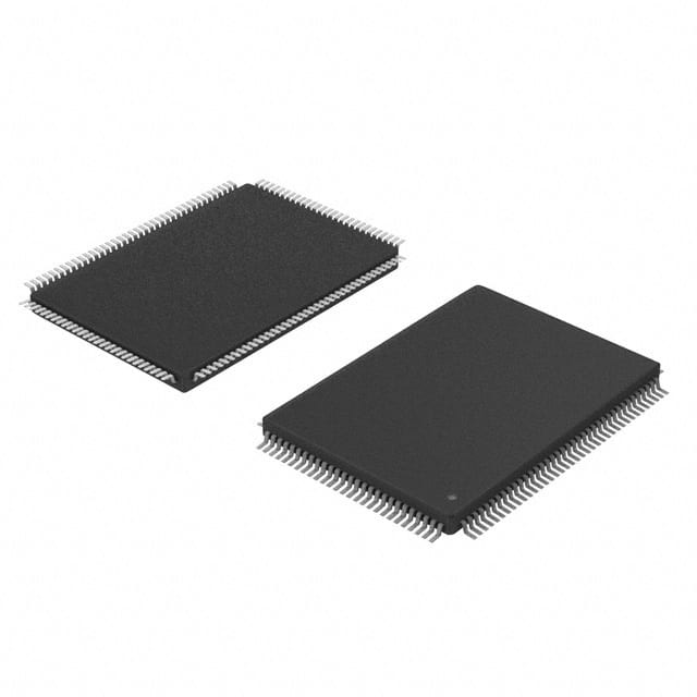
- Part No.:
- 82V2044EPFG8
- Manufacturer:
- Renesas
- Category:
- Telecom
- Package:
- 128-LQFP
- Datasheet:
-
 82V2044EPFG8.pdf
- Description:
- IC TELECOM INTERFACE 128TQFP
- Quantity:
- Payment:

- Shipping:

Inventory:3,387
Please send an inquiry. Send us your inquiry, and we will respond immediately.
Product details
Overview
IDT82V2044EPFG8 from Integrated Device Technology is a quad-channel T1/E1/J1 short-haul line interface unit (LIU) supporting simultaneous 4-channel line termination, clock/data recovery, AMI/B8ZS/HDB3 encoding/decoding, and adaptive equalization. It delivers -20 dB receive sensitivity, programmable per-channel line impedance (75 Ω, 100 Ω, 110 Ω, or 120 Ω), and integrated jitter attenuators placed in either transmit or receive path. Used in CSU/DSU equipment, wireless base stations, and IADs for telecom access networks.
For engineers reviewing the IDT82V2044EPFG8 datasheet, IDT82V2044EPFG8 pinout, IDT82V2044EPFG8 application, or IDT82V2044EPFG8 equivalent, key selection considerations include per-channel HPS support, G.772-compliant non-intrusive monitoring, JTAG boundary scan capability, 3.3 V single-supply operation with 5 V-tolerant I/O, and quad-channel PRBS/QRSS generation/detection with 215−1 (E1) and 220−1 (T1/J1) polynomials.
Technical Context
The IDT82V2044EPFG8 implements four independent T1/E1/J1 physical layer channels, each with configurable encoder/decoder, waveform shaper, adaptive equalizer, and dual-path jitter attenuator. Each channel supports software-selectable line encoding (B8ZS/HDB3/AMI), active-edge clocking, and programmable LOS detection thresholds.
It integrates dual control interfaces - parallel (Intel/Motorola non-multiplexed) and serial - plus JTAG test access port compliant with IEEE Std 1149.1. The device operates across industrial temperature range (−40°C to +85°C) and meets ANSI T1.102/T1.403/T1.408, ITU G.703/G.736/G.775/G.823, ETSI 300-166/300-233, and AT&T Pub 62411 standards.
Key Specifications
| Parameter | Value and Actual Design Meaning |
|---|---|
| Channels | 4 independent T1/E1/J1 line interfaces with full per-channel configuration |
| Line Encoding | B8ZS (T1/J1), HDB3 (E1), AMI (all); selectable per channel via register control |
| Receive Sensitivity | Up to −20 dB with adaptive equalizer enabled; supports long cable runs without external amplification |
| Jitter Attenuation | Per-channel jitter attenuator configurable in receive or transmit path; meets ITU G.823 jitter transfer requirements |
| LOS Detection | Programmable threshold per channel; adaptive equalizer enables dynamic adjustment of declare/clear criteria |
| Loopback Modes | Analog, digital, remote, and inband loopback - all configurable per channel for diagnostics and maintenance |
| PRBS/QRSS | 215−1 polynomial for E1; 220−1 for T1/J1; integrated generator/detector per channel with error counters |
| Power Supply | Single 3.3 V core supply (VDDD/VDDA/VDDR/VDDT/VDDIO); digital I/O pins tolerate up to 5 V |
Pinout & Package
Package: 128-pin TQFP (Thin Quad Flat Package), RoHS-compliant, body size 14 mm × 14 mm, 0.4 mm pitch.
| Pin/Terminal | Circuit Role | Design Meaning |
|---|---|---|
| TTIPn / TRINGn (n=1–4) | Differential line driver outputs | Transmit bipolar tip/ring outputs; individually or globally set to high-impedance via THZ pin or TCF1 register bit |
| RTIPn / RRINGn (n=1–4) | Differential line receiver inputs | Receive bipolar tip/ring inputs; support internal termination at 75 Ω, 100 Ω, 110 Ω, or 120 Ω per channel |
| TCLKn / RCLKn (n=1–4) | Channel clock inputs | Transmit/receive clock inputs; active edge programmable per channel (rising/falling) |
| TDn/TDPn / RDn/RDPn (n=1–4) | Data I/O | NRZ data interface in Single Rail mode; TDn sampled on TCLKn edge; RDn output on RCLKn edge |
| LOS1–LOS4 | Output | Per-channel Loss-of-Signal indicator; asserted low when signal loss detected per configured threshold |
| JTAG (TCK/TMS/TDI/TDO/TRST) | Test interface | IEEE 1149.1-compliant boundary scan; enables production testing and in-system debug without external hardware |
| CS/SCLK/SDI/SDO/INT | Serial control interface | 4-wire SPI-compatible interface; supports daisy-chaining multiple IDT82V2044EPFG8 devices |
| D[7:0]/A[7:0]/RD/WR/CS | Parallel control interface | Non-multiplexed Intel- or Motorola-style bus interface; enables direct microprocessor connection |
Key Features
| Feature | Design Value |
|---|---|
| HPS Support | Hitless Protection Switching for 1+1 redundancy without external relays - reduces failover latency and system complexity |
| Per-Channel Impedance Selection | Software-selectable line termination: 75 Ω (E1), 100 Ω (T1), 110 Ω (J1), or 120 Ω (E1) - eliminates BOM variants for multi-region deployments |
| G.772 Monitoring | Non-intrusive receive-line monitoring per ITU specification - enables live traffic analysis without service interruption |
| Short-Circuit Protection | Integrated line driver protection against sustained shorts - prevents latch-up and thermal damage during field faults |
| Waveform Programmability | User-definable arbitrary pulse shaping plus 5 preset templates - ensures compliance with regional line build-out requirements |
| PRBS/QRSS Diagnostics | On-chip pattern generation and detection with dedicated 16-bit BPV/excess-zero/PRBS/QRSS error counters - accelerates field commissioning and troubleshooting |
Applications
| CSU/DSU Equipment | Wireless Base Stations |
|---|---|
|
Use Scenario: Aggregating T1/E1 leased lines into backhaul transport for 2G/3G macrocells. IC Role / Device Role / Timing Role: Line interface unit performing clock/data recovery, line coding, and jitter attenuation for synchronous framer input. Use Value: Enables interoperability with legacy telco infrastructure while supporting HPS for carrier-grade uptime in remote cell sites. |
Use Scenario: Providing E1/T1 connectivity between BTS and BSC in distributed RAN architectures. IC Role / Device Role / Timing Role: Physical-layer interface converting bipolar line signals to NRZ data for framer or packet processor. Use Value: Reduces external component count by integrating adaptive equalization, loopbacks, and PRBS diagnostics - lowering board area and test cost. |
| IADs & Gateways | Routers & Frame Relay Access Devices |
|
Use Scenario: Supporting T1/E1 WAN uplinks in enterprise voice gateways handling SIP-to-PSTN translation. IC Role / Device Role / Timing Role: Short-haul LIU providing line termination, AIS/LOS detection, and G.772 monitoring for service assurance. Use Value: Allows real-time line health reporting to management systems without requiring protocol stack involvement. |
Use Scenario: Enabling E1-based frame relay access in branch office routers connecting to carrier POPs. IC Role / Device Role / Timing Role: Quad-channel line interface delivering synchronized data streams to HDLC controller with minimal jitter. Use Value: Per-channel jitter attenuator placement (RX/TX) maintains timing integrity across mixed-service traffic (voice + data). |
Equivalent & Alternatives
The following parts are listed as comparable options for similar line interface unit applications.
| Alternative Part | Technical Difference | Application Difference | Selection Advice |
|---|---|---|---|
| Maxim MAX3395E | Single-channel E1 LIU; no JTAG, no HPS, no adaptive equalizer; 5 V supply only | Limited to point-to-point E1 links without redundancy or long-cable compensation | Select when cost-sensitive, low-channel-count E1-only designs require minimal feature set |
| TI TLK2201BRGZR | Quad-channel 1.25 Gbps SerDes transceiver; no native T1/E1 encoding; requires external framer | Targets packet-based backhaul (e.g., CPRI, Ethernet), not TDM line interfacing | Select for high-speed serial transport where T1/E1 framing is handled upstream |
Compared with MAX3395E and TLK2201BRGZR, the IDT82V2044EPFG8 uniquely combines quad-channel T1/E1/J1 support, integrated HPS, adaptive equalization, and G.772 monitoring - making it the only option for carrier-class CSU/DSU and IAD designs requiring full standards compliance and field-diagnostic capability.
Availability
IDT82V2044EPFG8 is available at Aetrix Electronics and suitable for CSU/DSU equipment, wireless base station backhaul, and IAD gateway applications requiring stable component supply, long-lifecycle support, and industrial-temperature operation.
Supply support for IDT82V2044EPFG8 includes scheduled delivery planning, volume procurement assistance, BOM continuity management, traceable sourcing, and lifecycle availability coordination for OEM customers, industrial embedded developers, connected-device designers, and electronics production programs.
Manufacturer
Integrated Device Technology (IDT), now part of Renesas Electronics, is a fabless semiconductor company specializing in timing, memory interface, RF, and high-performance interconnect solutions for communications and computing markets.
The IDT82V2044EPFG8 belongs to IDT's legacy T1/E1/J1 line interface product line, designed specifically for telecom access equipment requiring multi-standard, multi-channel, and carrier-grade reliability in industrial environments.
FAQ
What standards does the IDT82V2044EPFG8 comply with?
The IDT82V2044EPFG8 complies with ANSI T1.102, T1.403, and T1.408; ITU-T I.431, G.703, G.736, G.775, and G.823; ETSI 300-166, 300-233, and TBR 12/13; and AT&T Pub 62411. These cover electrical, timing, jitter, and functional requirements for T1/E1/J1 short-haul line interfaces used in North America, Europe, and Japan.
Does the IDT82V2044EPFG8 support both T1 and E1 on the same device simultaneously?
Yes, the IDT82V2044EPFG8 supports per-channel T1, E1, or J1 configuration - all four channels can operate in mixed mode (e.g., two as T1, one as E1, one as J1). Line encoding (B8ZS/HDB3/AMI), impedance (75 Ω/100 Ω/110 Ω/120 Ω), and waveform templates are independently programmable per channel via registers.
How is Hitless Protection Switching (HPS) implemented in the IDT82V2044EPFG8?
The IDT82V2044EPFG8 implements HPS using internal switching logic that monitors primary and backup line signals, enabling sub-50 ms switchover without external relays or FPGA glue logic. The feature is enabled per channel via the HPS control register and requires no changes to PCB layout or external components.
What loopback modes does the IDT82V2044EPFG8 support, and how are they controlled?
The IDT82V2044EPFG8 supports analog, digital, remote, and inband loopback - all configurable per channel via dedicated control bits in MAINT0–MAINT5 registers. Inband loopback uses standard T1/E1 framing codes (e.g., 0x7F for E1) and can be activated/deactivated remotely without interrupting live traffic.
Is the IDT82V2044EPFG8 pin-compatible with earlier IDT82V2044 variants?
Yes, the IDT82V2044EPFG8 is pin-compatible with the IDT82V2044E (non-Pb-free) and IDT82V2044EPF (Pb-free, non-8 variant), sharing identical 128-pin TQFP footprint, pin functions, and register map. The "8" suffix denotes tape-and-reel packaging; electrical and functional behavior is identical across all versions.
82V2044EPFG8 Specifications
- Product attributes
- Attribute value
- Manufacturer:
- Renesas
- Series:
- -
- Package/Case:
- 128-LQFP
- Packaging:
- Tape & Reel (TR)
- Product Status:
- Obsolete
- Function:
- Transceiver
- Interface:
- LIU
- Number of Circuits:
- -
- Voltage - Supply:
- 3.13V ~ 3.47V
- Current - Supply:
- 55mA
- Power (Watts):
- -
- Operating Temperature:
- -40°C ~ 85°C
- Grade:
- -
- Qualification:
- -
- Mounting Type:
- Surface Mount
- Supplier Device Package:
- 128-TQFP (14x20)
82V2044EPFG8 FAQ
1.How can I place an order for 82V2044EPFG8 through Aetrix?
Please submit a Request for Quotation (RFQ) for 82V2044EPFG8 on Aetrix. Our sales agent will provide a competitive quotation and guide you through the order confirmation once you accept the terms.
2.Are the price and stock information for 82V2044EPFG8 reliable?
The price and inventory of 82V2044EPFG8 are updated periodically and may fluctuate due to market conditions. Stock and pricing data are typically refreshed every 24 hours. Quotation validity for 82V2044EPFG8 is usually 5 days.
3.What payment methods are accepted for 82V2044EPFG8?
We accept Wire Transfer, PayPal, Credit Card, Western Union, MoneyGram, and Escrow for 82V2044EPFG8 transactions.
Note: Certain payment methods may incur a processing fee.
4.How is shipping managed for 82V2044EPFG8?
82V2044EPFG8 orders can be shipped via leading logistics carriers, including DHL, UPS, FedEx, TNT, or Registered Mail.
Once your 82V2044EPFG8 order is processed, you will receive an email with the shipment details and tracking number.
Note: Tracking information may take up to 24 hours to appear. Express delivery typically takes 3–5 business days.
5.How can I obtain technical support or documentation for 82V2044EPFG8?
For technical support, including 82V2044EPFG8 datasheets, pinout diagrams, or application guidance, please contact our engineering support team. They can provide detailed documentation and assistance for your 82V2044EPFG8 requirements.
6.How does Aetrix verify that 82V2044EPFG8 is sourced from the original manufacturer or authorized distributors?
All 82V2044EPFG8 products on Aetrix are procured from qualified distributors and authorized channels. Our dedicated quality assurance team conducts strict verification, including traceability checks and, if necessary, third-party testing. This ensures that 82V2044EPFG8 meets industry standards.
7.What is the process for return or replacement of 82V2044EPFG8?
All 82V2044EPFG8 units undergo pre-shipment inspection (PSI). If there is an issue with 82V2044EPFG8, returns or replacements are accepted under the following conditions:
1.Quantity discrepancies, incorrect items, or visible external defects (such as breakage or corrosion), acknowledged by Aetrix.
2.The issue is reported within 90 days of delivery.
3.The 82V2044EPFG8 part is unused and in its original packaging.
Return procedure for 82V2044EPFG8:
1.Submit a request within 90 days.
2.Obtain a Return Material Authorization (RMA) from Aetrix.
82V2044EPFG8 Tags

-
LMC567CMX/NOPB
Texas Instruments
-
LM567CMX/NOPB
Texas Instruments
-
LM567CM/NOPB
Texas Instruments

-
VSC8531XMW-02
Microchip Technology
-
VSC8531XMW-05
Microchip Technology

-
GPY115C0VI
MaxLinear, Inc.

-
SI32185-A-FMR
Skyworks Solutions Inc.

-
VSC8541XMV-05
Microchip Technology

-
SI32178-B-FM1R
Skyworks Solutions Inc.
-
GPY215C0VI
MaxLinear, Inc.

-
CPC7514ZTR
Littelfuse Inc.

-
VSC8502XML-03
Microchip Technology
Tech Hub

TTL and CMOS logic families differ in thresholds, loading, output drive, power and timing. This engineering guide compares 74HC and 74HCT, calculates noise margins and checks 3.3 V/5 V compatibility.

A practical engineering guide to 3.3V and 5V logic compatibility, input thresholds, resistor dividers, translator ICs, MOSFET level shifting, I2C pull-ups, timing limits and power-sequencing risks.

The 74HC595 uses push-pull logic outputs, while the TPIC6B595 uses 50 V open-drain DMOS sinks for higher-power loads. This guide compares timing, current limits, 3.3 V interfacing, load wiring, thermal…

The 74HC595 converts serial data into eight stable parallel outputs. This guide covers pin functions, shift and storage timing, OE and MR behavior, drive-current limits, cascading, voltage compatibilit…

A technical comparison of level-sensitive latches and edge-triggered flip-flops, covering timing windows, setup and hold limits, master–slave operation, time borrowing, race-through, HDL inference and…

A D latch stores one bit while Enable controls when data can pass. This reference covers gate-level operation, truth tables, transparency, setup and hold timing, LE versus OE, common ICs and practical …

An SR latch stores one bit through cross-coupled feedback. This engineering reference covers NOR and NAND implementations, truth tables, forbidden-state recovery, gated operation, switch debouncing, fa…

Latch circuits retain one bit through feedback. This technical reference covers SR and D latches, truth tables, transparency, timing limits, latch-versus-flip-flop behavior, applications and common log…

An engineering guide to LED driver operation, constant-current and constant-voltage outputs, linear and switching topologies, dimming, IC selection, calculations, replacement compatibility, and fault c…

Operational amplifier guide covering op amp basics, feedback, ideal vs real op amps, common configurations, buffer circuits, offset, bias current, gain-bandwidth, slew rate, rail-to-rail limits and sel…


