
 My Inquiry
 My Account


Renesas 844004AKI-104LF
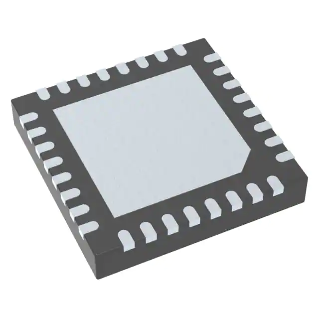
- Part No.:
- 844004AKI-104LF
- Manufacturer:
- Renesas
- Package:
- 32-VFQFN Exposed Pad
- Datasheet:
-
 844004AKI-104LF.pdf
- Description:
- IC FREQ SYNTH 32VFQFPN
- Quantity:
- Payment:

- Shipping:

Inventory:3,938
Please send an inquiry. Send us your inquiry, and we will respond immediately.
Product details
Overview
844004AKI-104LF from Integrated Device Technology is a 4-output LVDS frequency synthesizer optimized for Fibre Channel reference clock generation, using a 26.5625 MHz crystal to deliver selectable outputs of 212.5 MHz, 187.5 MHz, 159.375 MHz, 106.25 MHz, or 53.125 MHz via F_SEL[1:0] pins, with <1 ps typical RMS phase jitter (637 kHz–10 MHz) and 32-pin VFQFN packaging.
For engineers reviewing the 844004AKI-104LF datasheet, 844004AKI-104LF pinout, 844004AKI-104LF application, or 844004AKI-104LF equivalent, this device serves as a low-jitter crystal-to-LVDS clock source requiring precise frequency selection, differential output termination, and separate analog/core/output supply domains for high-integrity timing in storage and networking systems.
Technical Context
The 844004AKI-104LF integrates a third-generation low-phase-noise VCO (560–680 MHz range) with fixed M-divider (M = 24) and programmable N-divider (N = 2, 3, 4, 6, or 12), enabling five discrete output frequencies from a single crystal input. Its dual-reference architecture supports either crystal oscillator (XTAL_IN/XTAL_OUT) or single-ended LVCMOS/LVTTL REF_CLK input, selected by nXTAL_SEL.
It implements four independent LVDS output pairs (Q0/nQ0 through Q3/nQ3), each with matched rise/fall times (250–550 ps), tight output skew (<35 ps), and configurable 3.3 V or 2.5 V output supply (VDDO), while maintaining strict separation between VDD (core), VDDA (analog), and VDDO (output) rails to minimize supply-induced jitter.
Key Specifications
| Parameter | Value and Actual Design Meaning |
|---|---|
| Output count & type | 4 differential LVDS output pairs - enables simultaneous clock distribution to multiple high-speed receivers with common-mode noise rejection. |
| Output frequencies | 212.5 MHz, 187.5 MHz, 159.375 MHz, 106.25 MHz, 53.125 MHz - precisely aligned to Fibre Channel line rates and derived via integer-N division from crystal input. |
| RMS phase jitter | <0.75 ps typical (637 kHz–10 MHz) at 212.5 MHz - meets Fibre Channel jitter compliance without external filtering. |
| VCO range | 560 MHz–680 MHz - ensures stable lock across all five output frequencies with sufficient margin for PVT variation. |
| Supply configuration | Separate VDD (core), VDDA (analog PLL), VDDO (LVDS outputs) - isolates switching noise from sensitive analog circuitry to preserve jitter performance. |
| Operating temperature | −40°C to +85°C ambient - qualified for industrial and enterprise storage system environments. |
| Package | 32-pin VFQFN (5 mm × 5 mm × 0.925 mm, K package) - surface-mount footprint with exposed thermal pad for PCB-level heat dissipation. |
Pinout & Package
844004AKI-104LF is housed in a 32-pin Very Thin Quad Flat No-Lead (VFQFN) package with 0.5 mm pitch, 5 mm × 5 mm body, and exposed thermal pad (EPAD) requiring ground-connected vias per JEDEC MO-220 standards.
| Pin/Terminal | Circuit Role | Design Meaning |
|---|---|---|
| Q0, nQ0 / Q1, nQ1 / Q2, nQ2 / Q3, nQ3 | Differential LVDS outputs | Four independent true/inverted output pairs; each requires 100 Ω differential termination at receiver for signal integrity. |
| F_SEL0, F_SEL1 | Frequency select inputs | Pulldown-controlled logic pins selecting one of five output frequencies (00=212.5 MHz, 01=159.375 MHz, 10=106.25 MHz, 11=53.125 MHz, default=187.5 MHz). |
| MR | Active-HIGH master reset | Asynchronously resets internal dividers, forcing Qx low and nQx high; essential for deterministic startup and fault recovery. |
| nPLL_SEL | PLL enable/bypass control | When LOW, enables PLL path; when HIGH, bypasses PLL and routes REF_CLK directly to dividers - supports clock redundancy. |
| nXTAL_SEL | Reference source selector | When LOW, selects XTAL_IN/XTAL_OUT; when HIGH, selects REF_CLK - enables flexible clock sourcing without hardware change. |
| VDD, VDDA, VDDO, GND | Power domain supplies | VDD (core logic), VDDA (PLL/analog), VDDO (LVDS drivers), and dual GND pins must be decoupled independently with 0.01 µF + 10 µF (VDDA) capacitors. |
| XTAL_IN, XTAL_OUT | Crystal oscillator interface | Designed for 18 pF parallel-resonant crystals (e.g., 26.5625 MHz); internal load caps eliminate need for external tuning components. |
| REF_CLK | Single-ended reference input | LVTTL/LVCMOS-compatible input accepting 23.4375–28.33 MHz signals; used when crystal is unavailable or system requires external clock source. |
Key Features
| Feature | Design Value |
|---|---|
| Crystal-to-LVDS synthesis | Direct conversion of 26.5625 MHz crystal into five Fibre Channel–aligned LVDS clocks without external PLL or buffer stages. |
| Multi-supply domain isolation | Dedicated VDD (core), VDDA (analog), and VDDO (outputs) rails prevent digital switching noise from degrading PLL phase noise performance. |
| Configurable reference input | Supports both crystal (XTAL_IN/XTAL_OUT) and single-ended LVCMOS/LVTTL (REF_CLK) sources, selected dynamically via nXTAL_SEL pin. |
| Low-jitter VCO architecture | IDT's 3rd-generation VCO achieves <0.75 ps RMS jitter at 212.5 MHz - eliminates need for external jitter cleaners in FC-PI-4/FC-PI-5 designs. |
| Industrial temperature operation | Guaranteed functionality from −40°C to +85°C ambient with full AC/DC specs - suitable for uncooled rack-mounted storage controllers. |
Applications
| Fibre Channel Storage Controllers | Enterprise RAID Systems |
|---|---|
Use Scenario: Generating synchronized 212.5 MHz and 106.25 MHz reference clocks for FC-PI-4/FC-PI-5 SerDes lanes in host bus adapters and switch fabric interfaces. IC Role / Device Role / Timing Role: Primary clock synthesizer converting a single crystal into multiple low-jitter LVDS clocks distributed to transceiver PHYs and link-layer logic. Use Value: Eliminates discrete clock trees and reduces BOM count while meeting FC jitter mask requirements without post-synthesis filtering. |
Use Scenario: Providing redundant 187.5 MHz and 159.375 MHz clocks to dual-controller RAID modules with failover capability. IC Role / Device Role / Timing Role: Dual-role timing IC supporting both primary clock generation and PLL-bypass mode for reference clock switchover during controller failover. Use Value: Enables seamless clock source transition with sub-ns skew between active and standby paths, preserving data coherency during redundancy events. |
| High-Speed Data Acquisition Backplanes | Optical Transport Network Line Cards |
Use Scenario: Delivering matched 106.25 MHz and 53.125 MHz clocks to ADC/DAC clock domains and FPGA fabric in modular test equipment. IC Role / Device Role / Timing Role: Multi-frequency clock source with deterministic inter-output skew (<35 ps) for time-aligned sampling and processing pipelines. Use Value: Ensures sub-cycle timing alignment across mixed-signal subsystems, reducing aperture uncertainty and improving effective resolution. |
Use Scenario: Supplying 212.5 MHz and 159.375 MHz LVDS clocks to OTU2/OTU1 framer ASICs and forward error correction engines in DWDM line cards. IC Role / Device Role / Timing Role: Jitter-compliant clock generator meeting ITU-T G.823/G.824 wander and jitter limits for synchronous optical networking. Use Value: Achieves <0.75 ps RMS jitter at 212.5 MHz - exceeds OC-48/STM-16 timing stability requirements without external VCXO or DCO support. |
Equivalent & Alternatives
The following parts are listed as comparable options for similar crystal-to-LVDS frequency synthesizer applications.
| Alternative Part | Technical Difference | Application Difference | Selection Advice |
|---|---|---|---|
| Si5338A-A-GM | Programmable I2C-based clock generator with wider output frequency range (0.16–350 MHz), higher integration (4 outputs, integrated EEPROM), but higher typical jitter (0.9 ps @ 156.25 MHz). | Used where field-programmability and multi-protocol support (Ethernet, CPRI, PCIe) are required instead of fixed Fibre Channel frequencies. | Select Si5338A-A-GM if design requires dynamic reconfiguration or support for non-Fibre Channel protocols; not drop-in compatible due to different pinout and control interface. |
| ICS8442I-104 | Same family, 2-output variant with identical VCO, jitter performance, and pin-compatible footprint (32-pin VFQFN), but only two LVDS output pairs and no F_SEL[1:0] pins. | Applied in cost-sensitive or space-constrained designs needing only two synchronized clocks (e.g., dual-lane FC interfaces). | Choose ICS8442I-104 when exactly two outputs suffice and board layout reuse is prioritized; shares same thermal and power design rules as 844004AKI-104LF. |
Compared with Si5338A-A-GM and ICS8442I-104, the 844004AKI-104LF delivers superior jitter performance at Fibre Channel frequencies with zero software overhead, while offering pin-compatible scalability within the ICS844xx family - making it optimal for fixed-function, high-reliability storage timing.
Availability
844004AKI-104LF is available at Aetrix Electronics and suitable for Fibre Channel storage controllers, enterprise RAID systems, high-speed data acquisition backplanes, and optical transport network line cards requiring stable component supply across long production lifecycles.
Supply support for 844004AKI-104LF includes scheduled delivery planning, volume procurement assistance, BOM continuity management, traceable sourcing, and lifecycle availability coordination for OEM customers, industrial embedded developers, connected-device designers, and electronics production programs.
Manufacturer
Integrated Device Technology (IDT), now part of Renesas Electronics, is a fabless semiconductor company specializing in timing, memory interface, RF, and sensor solutions for communications, computing, and industrial markets.
The 844004AKI-104LF belongs to IDT's FemtoClock® family of ultra-low-jitter clock synthesizers, designed specifically to replace crystal oscillators and discrete PLLs in high-speed serial interface timing applications including Fibre Channel, SAS, and OTN.
FAQ
What crystal frequency and load capacitance is required for 844004AKI-104LF?
The 844004AKI-104LF is characterized for use with a 26.5625 MHz, 18 pF parallel-resonant crystal. It supports alternative crystals from 23.33 MHz to 28.33 MHz, but optimal jitter and frequency accuracy are achieved with the specified 18 pF value. The device includes internal load capacitance, eliminating need for external C1/C2 tuning capacitors in most layouts.
Can 844004AKI-104LF operate with a 2.5 V supply instead of 3.3 V?
Yes, the 844004AKI-104LF supports dual supply modes: full 3.3 V (±5%) or full 2.5 V (±5%) operation across VDD, VDDA, and VDDO. At 2.5 V, LVDS output voltage swing reduces to 250–550 mV differential, and RMS phase jitter increases slightly (e.g., 0.74 ps at 187.5 MHz), remaining well within Fibre Channel specifications.
How is output frequency selected on 844004AKI-104LF?
Output frequency is selected via the F_SEL[1:0] pins (pins 10 and 12), which are internally pulldown. Logic states 00, 01, 10, and 11 configure the N-divider to produce 212.5 MHz, 159.375 MHz, 106.25 MHz, and 53.125 MHz respectively. The default 187.5 MHz output occurs when a 23.4375 MHz crystal is used with F_SEL[1:0] = 00.
Does 844004AKI-104LF require external termination for its LVDS outputs?
Yes, each LVDS output pair (e.g., Q0/nQ0) must be terminated with a 100 Ω differential resistor at the receiver end. The 844004AKI-104LF does not integrate termination; leaving outputs unterminated or improperly terminated causes reflections, increased jitter, and signal integrity failure - especially critical above 100 MHz.
What is the function of the nPLL_SEL pin on 844004AKI-104LF?
The nPLL_SEL pin (pin 4) controls whether the internal PLL is active. When LOW, the PLL is enabled and the VCO synthesizes output frequencies from the reference input. When HIGH, the PLL is bypassed and the reference clock (crystal or REF_CLK) passes directly to the output dividers - enabling transparent clock forwarding for redundancy or test modes.
844004AKI-104LF Specifications
- Product attributes
- Attribute value
- Manufacturer:
- Renesas
- Series:
- FemtoClock®
- Package/Case:
- 32-VFQFN Exposed Pad
- Packaging:
- Tray
- Product Status:
- Obsolete
- Programmable:
- Not Verified
- Type:
- Frequency Synthesizer
- PLL:
- Yes with Bypass
- Input:
- LVCMOS, LVTTL, Crystal
- Output:
- LVDS
- Number of Circuits:
- 1
- Ratio - Input:Output:
- 2:4
- Differential - Input:Output:
- No/Yes
- Frequency - Max:
- 226.66MHz
- Divider/Multiplier:
- Yes/No
- Voltage - Supply:
- 2.375V ~ 3.465V
- Operating Temperature:
- -40°C ~ 85°C
- Mounting Type:
- Surface Mount
- Grade:
- -
- Qualification:
- -
- Supplier Device Package:
- 32-VFQFPN (5x5)
844004AKI-104LF FAQ
1.How can I place an order for 844004AKI-104LF through Aetrix?
Please submit a Request for Quotation (RFQ) for 844004AKI-104LF on Aetrix. Our sales agent will provide a competitive quotation and guide you through the order confirmation once you accept the terms.
2.Are the price and stock information for 844004AKI-104LF reliable?
The price and inventory of 844004AKI-104LF are updated periodically and may fluctuate due to market conditions. Stock and pricing data are typically refreshed every 24 hours. Quotation validity for 844004AKI-104LF is usually 5 days.
3.What payment methods are accepted for 844004AKI-104LF?
We accept Wire Transfer, PayPal, Credit Card, Western Union, MoneyGram, and Escrow for 844004AKI-104LF transactions.
Note: Certain payment methods may incur a processing fee.
4.How is shipping managed for 844004AKI-104LF?
844004AKI-104LF orders can be shipped via leading logistics carriers, including DHL, UPS, FedEx, TNT, or Registered Mail.
Once your 844004AKI-104LF order is processed, you will receive an email with the shipment details and tracking number.
Note: Tracking information may take up to 24 hours to appear. Express delivery typically takes 3–5 business days.
5.How can I obtain technical support or documentation for 844004AKI-104LF?
For technical support, including 844004AKI-104LF datasheets, pinout diagrams, or application guidance, please contact our engineering support team. They can provide detailed documentation and assistance for your 844004AKI-104LF requirements.
6.How does Aetrix verify that 844004AKI-104LF is sourced from the original manufacturer or authorized distributors?
All 844004AKI-104LF products on Aetrix are procured from qualified distributors and authorized channels. Our dedicated quality assurance team conducts strict verification, including traceability checks and, if necessary, third-party testing. This ensures that 844004AKI-104LF meets industry standards.
7.What is the process for return or replacement of 844004AKI-104LF?
All 844004AKI-104LF units undergo pre-shipment inspection (PSI). If there is an issue with 844004AKI-104LF, returns or replacements are accepted under the following conditions:
1.Quantity discrepancies, incorrect items, or visible external defects (such as breakage or corrosion), acknowledged by Aetrix.
2.The issue is reported within 90 days of delivery.
3.The 844004AKI-104LF part is unused and in its original packaging.
Return procedure for 844004AKI-104LF:
1.Submit a request within 90 days.
2.Obtain a Return Material Authorization (RMA) from Aetrix.
844004AKI-104LF Tags

-
CD74HCT4046AM96
Texas Instruments

-
MC14046BDWR2G
onsemi

-
501MILFT
Renesas
-
CD74HC7046AM
Texas Instruments

-
CDCVF2505PWR
Texas Instruments

-
RC19004A100GNL#KB0
Renesas

-
SI5351A-B-GTR
Skyworks Solutions Inc.

-
CY2305SXI-1T
Infineon Technologies
-
570BILFT
Renesas

-
CDCE913PWR
Texas Instruments
-
CY2305SXI-1HT
Infineon Technologies

-
DS1086LU+T
Analog Devices Inc./Maxim Integrated
Tech Hub

TTL and CMOS logic families differ in thresholds, loading, output drive, power and timing. This engineering guide compares 74HC and 74HCT, calculates noise margins and checks 3.3 V/5 V compatibility.

A practical engineering guide to 3.3V and 5V logic compatibility, input thresholds, resistor dividers, translator ICs, MOSFET level shifting, I2C pull-ups, timing limits and power-sequencing risks.

The 74HC595 uses push-pull logic outputs, while the TPIC6B595 uses 50 V open-drain DMOS sinks for higher-power loads. This guide compares timing, current limits, 3.3 V interfacing, load wiring, thermal…

The 74HC595 converts serial data into eight stable parallel outputs. This guide covers pin functions, shift and storage timing, OE and MR behavior, drive-current limits, cascading, voltage compatibilit…

A technical comparison of level-sensitive latches and edge-triggered flip-flops, covering timing windows, setup and hold limits, master–slave operation, time borrowing, race-through, HDL inference and…

A D latch stores one bit while Enable controls when data can pass. This reference covers gate-level operation, truth tables, transparency, setup and hold timing, LE versus OE, common ICs and practical …

An SR latch stores one bit through cross-coupled feedback. This engineering reference covers NOR and NAND implementations, truth tables, forbidden-state recovery, gated operation, switch debouncing, fa…

Latch circuits retain one bit through feedback. This technical reference covers SR and D latches, truth tables, transparency, timing limits, latch-versus-flip-flop behavior, applications and common log…

An engineering guide to LED driver operation, constant-current and constant-voltage outputs, linear and switching topologies, dimming, IC selection, calculations, replacement compatibility, and fault c…

Operational amplifier guide covering op amp basics, feedback, ideal vs real op amps, common configurations, buffer circuits, offset, bias current, gain-bandwidth, slew rate, rail-to-rail limits and sel…


