
 My Inquiry
 My Account


Renesas 854S202AYILF
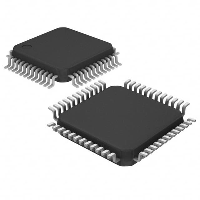
- Part No.:
- 854S202AYILF
- Manufacturer:
- Renesas
- Category:
- Clock Buffers, Drivers
- Package:
- 48-LQFP
- Datasheet:
-
 854S202AYILF.pdf
- Description:
- IC CLK MULTIPLX 12:2 3GHZ 48TQFP
- Quantity:
- Payment:

- Shipping:

Inventory:2,979
Please send an inquiry. Send us your inquiry, and we will respond immediately.
Product details
Overview
854S202AYILF from Renesas Electronics (formerly IDT) is a 12:2 differential-to-LVDS clock multiplexer with dual 3.3V LVDS outputs, twelve selectable differential inputs (LVPECL/LVDS/CML compatible), and guaranteed operation up to 3GHz. It delivers ultra-low skew-50ps max output skew, 100ps max input skew-and 0.16ps typical additive phase jitter (12kHz–20MHz), making it suitable for high-speed serial link timing distribution in telecom infrastructure and FPGA-based test equipment.
For engineers reviewing the 854S202AYILF datasheet, 854S202AYILF pinout, 854S202AYILF application, or 854S202AYILF equivalent, key selection criteria include differential input level flexibility, sub-1.1ns propagation delay, part-to-part skew ≤250ps, LVDS output compliance, and support for independent bank-selectable routing of any input to QA/nQA or QB/nQB outputs under industrial temperature range (−40°C to +85°C).
Technical Context
The 854S202AYILF implements a fully differential signal path with separate 4-bit control buses (SELA_[3:0] and SELB_[3:0]) enabling independent selection of one of twelve differential clock inputs per LVDS output pair. Its architecture supports simultaneous operation of both banks with no inter-bank crosstalk degradation beyond specified MUX isolation (≥75dB at <1.2GHz).
Each CLKx/nCLKx input pair accepts LVPECL, LVDS, or CML signals via internal biasing (VDD/2 default on floating nCLKx), while OEA/OEB pins provide independent LVCMOS/LVTTL-controlled enable/disable of QA/nQA and QB/nQB outputs. Propagation delay is frequency-dependent (≤900ps at >2GHz), and output duty cycle remains within 40–60% across full operating conditions.
Key Specifications
| Parameter | Value and Actual Design Meaning |
|---|---|
| Max Output Frequency | 3 GHz - supports PCIe Gen4, 10G/25G Ethernet, and SerDes reference clock distribution |
| Propagation Delay | ≤900 ps at >2 GHz - ensures tight timing alignment in multi-channel high-speed systems |
| Output Skew (max) | 50 ps - guarantees matched edge timing between QA/nQA and QB/nQB for synchronous sampling |
| Additive Phase Jitter (RMS) | 0.16 ps (12 kHz–20 MHz) - meets stringent jitter budgets for serial data recovery circuits |
| Input Level Compatibility | LVPECL / LVDS / CML - eliminates need for external level-shifting circuitry in mixed-signal clock trees |
| Supply Voltage | 3.3 V ±5% - aligns with standard I/O voltage domains in modern FPGA and ASIC platforms |
| Ambient Temp Range | −40°C to +85°C - qualified for industrial and telecom base station environments |
Pinout & Package
854S202AYILF is housed in a lead-free 48-pin LQFP package (7 mm × 7 mm × 1.4 mm, Y suffix), with exposed thermal pad not electrically connected. Power and ground pins are distributed across all four sides for low-inductance decoupling; differential I/Os are arranged to minimize coupling between adjacent pairs.
| Pin/Terminal | Circuit Role | Design Meaning |
|---|---|---|
| CLK0–CLK11, nCLK0–nCLK11 | Differential clock inputs (12 pairs) | Accept LVPECL/LVDS/CML; internal pullup/pulldown enables safe floating; VDD/2 common-mode default on nCLKx |
| QA, nQA / QB, nQB | Differential LVDS outputs (2 pairs) | 3.3V LVDS-compliant; 247–454 mV differential swing; 1.2–1.4 V offset voltage |
| SELA_[3:0], SELB_[3:0] | Bank A/B input select controls | LVCMOS/LVTTL logic; 4-bit binary encoding selects one of 12 inputs per output bank |
| OEA, OEB | Output enable (active-high) | Individually disables QA/nQA or QB/nQB; internal pullup ensures default-enabled state if left unconnected |
| VDD (pins 5,18,32,43) | Power supply | Four dedicated 3.3V supply pins reduce IR drop and improve PSRR across high-frequency operation |
| GND (pins 6,8,15,22,29,39,46) | Ground return | Seven ground pins provide low-impedance return paths for both core logic and LVDS drivers |
Key Features
| Feature | Design Value |
|---|---|
| Independent dual-bank multiplexing | SELA_[3:0] and SELB_[3:0] allow concurrent, non-interfering routing of different inputs to QA/nQA and QB/nQB |
| Multi-standard differential input support | Single device replaces discrete level translators when interfacing LVPECL clocks to LVDS receivers |
| Ultra-low deterministic jitter | 0.16ps RMS additive phase jitter enables use in <100 fs total jitter budget applications (e.g., 25G KR) |
| Industrial temperature qualification | Full parameter guarantee from −40°C to +85°C ambient without derating - suitable for uncooled outdoor equipment |
| Robust unused pin handling | All control and clock inputs have defined internal terminations; floating CLK/nCLK pairs are electrically safe per datasheet guidance |
Applications
| 5G Radio Unit Synchronization | High-Speed Test Equipment Clock Tree |
|---|---|
Use Scenario: Distributing synchronized reference clocks across multiple RF transceivers and ADC/DAC arrays in active antenna systems. IC Role / Device Role / Timing Role: 12:2 multiplexer routes GPS-disciplined OCXO or atomic clock signals to two independent beamforming chains with matched latency. Use Value: Sub-50ps output skew ensures phase-coherent sampling across distributed converters, directly supporting 3GPP FR2 phase alignment requirements. |
Use Scenario: Providing switchable, low-jitter clock sources to multiple DUT interfaces (e.g., JESD204B, PCIe, SATA) within automated test fixtures. IC Role / Device Role / Timing Role: Central clock router selecting among calibrated lab-grade oscillators (100MHz, 156.25MHz, 312.5MHz) for stimulus generation and capture timing. Use Value: 0.16ps jitter preserves signal integrity during high-resolution eye diagram measurements, reducing false failure rates in production testing. |
| FPGA-Based Protocol Analyzer | Optical Transport Network Line Card |
Use Scenario: Feeding parallel high-speed SerDes lanes (e.g., 28G PAM4) in real-time packet inspection hardware with dynamic clock source switching. IC Role / Device Role / Timing Role: Dual-output multiplexer supplies independent clocks to FPGA transceiver banks and embedded processor subsystems, each selectable from shared 12-input pool. Use Value: Independent OEA/OEB enables glitch-free clock domain gating during protocol handshakes, preventing metastability in time-critical control paths. |
Use Scenario: Clock distribution in OTU4/OTU3 line cards requiring redundant, swappable timing sources for SONET/SDH framers and FEC engines. IC Role / Device Role / Timing Role: Fault-tolerant clock selector routing primary and backup BITS/SSU inputs to dual LVDS fanout buffers with automatic failover capability. Use Value: Part-to-part skew ≤250ps allows seamless switchover between timing sources without disrupting frame alignment in 100G coherent optics subsystems. |
Equivalent & Alternatives
The following parts are listed as comparable options for similar differential clock multiplexer applications.
| Alternative Part | Technical Difference | Application Difference | Selection Advice |
|---|---|---|---|
| PI6C557-03BLE | 8:2 LVDS mux; max 2.5GHz; 0.25ps jitter; only LVDS inputs | Limited input standard support; lower channel count; higher jitter floor | Choose when system uses only LVDS sources and requires lower cost, smaller footprint (32-QFN) |
| SI53302-A-GM | 2:2 universal buffer/mux; programmable via I²C; 0.18ps jitter; supports LVDS/LVPECL/CML | Requires configuration firmware; lacks independent bank enables; higher power (160mA) | Prefer when dynamic reconfiguration or multi-function flexibility (buffer/mux/divider) is required over static routing simplicity |
Compared with PI6C557-03BLE and SI53302-A-GM, the 854S202AYILF provides the highest input channel density (12), lowest guaranteed output skew (50ps), and simplest pin-strapped control-making it optimal for fixed-architecture, high-channel-count clock distribution where deterministic latency and minimal BOM count are critical.
Availability
854S202AYILF is available at Aetrix Electronics and suitable for 5G infrastructure, high-speed test equipment, and optical transport network line cards requiring stable component supply across extended product lifecycles.
Supply support for 854S202AYILF includes scheduled delivery planning, volume procurement assistance, BOM continuity management, traceable sourcing, and lifecycle availability coordination for OEM customers, industrial embedded developers, connected-device designers, and electronics production programs.
Manufacturer
Renesas Electronics Corporation is a global semiconductor leader delivering trusted embedded solutions for automotive, industrial, infrastructure, and IoT applications.
The 854S202AYILF belongs to Renesas' high-performance timing portfolio, designed specifically for low-skew, multi-source clock distribution in next-generation wired and wireless communication systems.
FAQ
What input voltage levels does the 854S202AYILF support on its CLK/nCLK pins?
The 854S202AYILF accepts LVPECL, LVDS, and CML differential input levels on all twelve CLKx/nCLKx pairs. Input common-mode range is GND + 0.5V to VDD – 0.7V (2.8V to 2.6V at 3.3V supply), and peak-to-peak swing must be 0.15V–1.5V. Internal pullup/pulldown resistors (51kΩ typical) set default bias at VDD/2 when nCLKx is floating, enabling safe single-ended interface adaptation per datasheet Figure 1.
How is output enable controlled on the 854S202AYILF?
The 854S202AYILF uses two dedicated LVCMOS/LVTTL-compatible enable pins: OEA controls QA/nQA, and OEB controls QB/nQB. Both are active-high with internal pullup resistors, so outputs remain enabled by default if left unconnected. Driving either pin low disables its respective LVDS output pair, presenting high-impedance differential states-critical for hot-swap and power-gating scenarios in modular systems.
Does the 854S202AYILF require external termination resistors on its LVDS outputs?
No external termination is required on the 854S202AYILF's LVDS outputs. The device drives into standard 100Ω differential loads, and its output stage is designed to meet LVDS specifications (247–454mV differential swing, 1.2–1.4V common-mode) without added series or parallel components. However, PCB layout must maintain controlled 100Ω differential impedance and place matching termination at the receiver end per JEDEC standards.
What is the maximum guaranteed propagation delay for the 854S202AYILF at 2.5GHz?
At 2.5GHz output frequency, the 854S202AYILF guarantees a maximum propagation delay of 900ps (tpLH and tpHL), as specified in Table 5 for fOUT > 2GHz. This value includes worst-case process/voltage/temperature corners and accounts for both rising and falling edges, ensuring predictable timing margins in high-speed clock tree design.
Can the 854S202AYILF operate with only six of its twelve inputs used?
Yes-the 854S202AYILF supports partial input utilization. Unused CLKx/nCLKx pairs may be left floating per datasheet guidance (Section "Recommendations for Unused Input and Output Pins"), as each nCLKx pin has an internal pullup/pulldown that sets VDD/2 common-mode bias. No external resistors are required, though a 1kΩ resistor to ground on unused CLKx pins is optional for ESD robustness.
854S202AYILF Specifications
- Product attributes
- Attribute value
- Manufacturer:
- Renesas
- Series:
- -
- Package/Case:
- 48-LQFP
- Packaging:
- Bulk
- Product Status:
- Obsolete
- Type:
- Multiplexer
- Number of Circuits:
- 1
- Ratio - Input:Output:
- 12:2
- Differential - Input:Output:
- Yes/Yes
- Input:
- HCSL, HSTL, LVDS, LVPECL, SSTL
- Output:
- LVDS
- Frequency - Max:
- 3 GHz
- Voltage - Supply:
- 3.135V ~ 3.465V
- Operating Temperature:
- -40°C ~ 85°C
- Mounting Type:
- Surface Mount
- Grade:
- -
- Qualification:
- -
- Supplier Device Package:
- 48-TQFP (7x7)
854S202AYILF FAQ
1.How can I place an order for 854S202AYILF through Aetrix?
Please submit a Request for Quotation (RFQ) for 854S202AYILF on Aetrix. Our sales agent will provide a competitive quotation and guide you through the order confirmation once you accept the terms.
2.Are the price and stock information for 854S202AYILF reliable?
The price and inventory of 854S202AYILF are updated periodically and may fluctuate due to market conditions. Stock and pricing data are typically refreshed every 24 hours. Quotation validity for 854S202AYILF is usually 5 days.
3.What payment methods are accepted for 854S202AYILF?
We accept Wire Transfer, PayPal, Credit Card, Western Union, MoneyGram, and Escrow for 854S202AYILF transactions.
Note: Certain payment methods may incur a processing fee.
4.How is shipping managed for 854S202AYILF?
854S202AYILF orders can be shipped via leading logistics carriers, including DHL, UPS, FedEx, TNT, or Registered Mail.
Once your 854S202AYILF order is processed, you will receive an email with the shipment details and tracking number.
Note: Tracking information may take up to 24 hours to appear. Express delivery typically takes 3–5 business days.
5.How can I obtain technical support or documentation for 854S202AYILF?
For technical support, including 854S202AYILF datasheets, pinout diagrams, or application guidance, please contact our engineering support team. They can provide detailed documentation and assistance for your 854S202AYILF requirements.
6.How does Aetrix verify that 854S202AYILF is sourced from the original manufacturer or authorized distributors?
All 854S202AYILF products on Aetrix are procured from qualified distributors and authorized channels. Our dedicated quality assurance team conducts strict verification, including traceability checks and, if necessary, third-party testing. This ensures that 854S202AYILF meets industry standards.
7.What is the process for return or replacement of 854S202AYILF?
All 854S202AYILF units undergo pre-shipment inspection (PSI). If there is an issue with 854S202AYILF, returns or replacements are accepted under the following conditions:
1.Quantity discrepancies, incorrect items, or visible external defects (such as breakage or corrosion), acknowledged by Aetrix.
2.The issue is reported within 90 days of delivery.
3.The 854S202AYILF part is unused and in its original packaging.
Return procedure for 854S202AYILF:
1.Submit a request within 90 days.
2.Obtain a Return Material Authorization (RMA) from Aetrix.
854S202AYILF Tags

-
PL133-37TC-R
Microchip Technology
-
PL133-27GC-R
Microchip Technology
-
LMK1C1102DQFR
Texas Instruments

-
LMK1C1102PWR
Texas Instruments
-
LMK1C1104DQFR
Texas Instruments
-
LMK1C1104PWR
Texas Instruments
-
CDC3RL02YFPR
Texas Instruments

-
SY75602ATWL-TR
Microchip Technology
-
SY75603ATWL-TR
Microchip Technology
-
5PB1102CMGI8
Renesas
-
PL133-27GI-R
Microchip Technology

-
551MLFT
Renesas
Tech Hub

TTL and CMOS logic families differ in thresholds, loading, output drive, power and timing. This engineering guide compares 74HC and 74HCT, calculates noise margins and checks 3.3 V/5 V compatibility.

A practical engineering guide to 3.3V and 5V logic compatibility, input thresholds, resistor dividers, translator ICs, MOSFET level shifting, I2C pull-ups, timing limits and power-sequencing risks.

The 74HC595 uses push-pull logic outputs, while the TPIC6B595 uses 50 V open-drain DMOS sinks for higher-power loads. This guide compares timing, current limits, 3.3 V interfacing, load wiring, thermal…

The 74HC595 converts serial data into eight stable parallel outputs. This guide covers pin functions, shift and storage timing, OE and MR behavior, drive-current limits, cascading, voltage compatibilit…

A technical comparison of level-sensitive latches and edge-triggered flip-flops, covering timing windows, setup and hold limits, master–slave operation, time borrowing, race-through, HDL inference and…

A D latch stores one bit while Enable controls when data can pass. This reference covers gate-level operation, truth tables, transparency, setup and hold timing, LE versus OE, common ICs and practical …

An SR latch stores one bit through cross-coupled feedback. This engineering reference covers NOR and NAND implementations, truth tables, forbidden-state recovery, gated operation, switch debouncing, fa…

Latch circuits retain one bit through feedback. This technical reference covers SR and D latches, truth tables, transparency, timing limits, latch-versus-flip-flop behavior, applications and common log…

An engineering guide to LED driver operation, constant-current and constant-voltage outputs, linear and switching topologies, dimming, IC selection, calculations, replacement compatibility, and fault c…

Operational amplifier guide covering op amp basics, feedback, ideal vs real op amps, common configurations, buffer circuits, offset, bias current, gain-bandwidth, slew rate, rail-to-rail limits and sel…


