
 My Inquiry
 My Account


Renesas 89H32H8G3YCHLGI
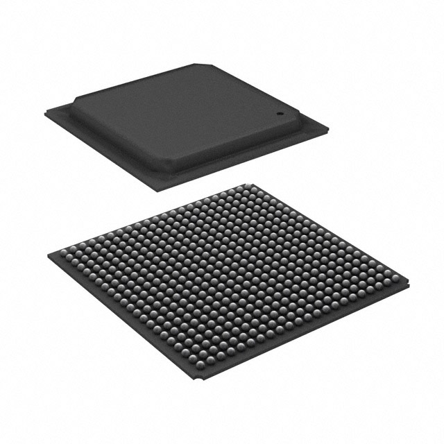
- Part No.:
- 89H32H8G3YCHLGI
- Manufacturer:
- Renesas
- Category:
- Specialized
- Package:
- 484-BBGA, FCBGA
- Datasheet:
-
 89H32H8G3YCHLGI.pdf
- Description:
- IC INTFACE SPECIALIZED 484FCBGA
- Quantity:
- Payment:

- Shipping:

Inventory:2,849
Please send an inquiry. Send us your inquiry, and we will respond immediately.
Product details
Overview
The 89H32H8G3 from IDT is a 32-lane, 8-port PCI Express Gen3 system interconnect switch with non-blocking architecture, integrated SerDes supporting 8.0 GT/s, 64 GBps switching capacity, and full PCIe Base Specification 3.0 compliance - deployed in enterprise servers for CPU-to-IO expansion and multi-root partitioning.
For engineers reviewing the 89H32H8G3 datasheet, 89H32H8G3 pinout, 89H32H8G3 application, or 89H32H8G3 equivalent, key selection criteria include Gen3 lane aggregation (x8/x4/x2/x1 per port), SECDED ECC on internal RAMs, AER support across all ports, hot-plug capability on downstream ports, and autonomous link width negotiation.
Technical Context
This device implements a cut-through, low-latency PCIe Gen3 switch core with frame buffer, route table, scheduler, and port arbitration logic - enabling concurrent peer-to-peer traffic flows across up to eight independent partitions. It integrates four DL/Transaction Layer blocks, each paired with SerDes supporting x8/x4/x2/x1 configurations.
It supports full PCIe 3.0 optional features including Advanced Error Reporting (AER), Access Control Services (ACS), Atomic Operations, Latency Tolerance Reporting (LTR), and Optimized Buffer Flush/Fill (OBFF), alongside D0/D3hot/D3 power states and Active State Power Management (ASPM).
Key Specifications
| Parameter | Value and Actual Design Meaning |
|---|---|
| Lane Count | 32 total PCIe lanes - configurable as up to four x8 ports or eight x4 ports for flexible topology mapping. |
| Data Rate | 8.0 GT/s per lane (PCIe Gen3) - delivers 256 Gbps full-duplex aggregate bandwidth (32 GBps). |
| Compliance | PCI Express Base Specification 3.0 - includes mandatory and optional features (AER, ACS, ARI, LTR, OBFF). |
| Error Handling | SECDED ECC on all internal RAMs + end-to-end data path parity - enables robust RAS in mission-critical server environments. |
| Power States | Supports D0, D3hot, D3 - with ASPM L0s/L1 entry/exit controlled per port for dynamic power optimization. |
| Initialization | Multiple boot sources: BIOS/OS/driver, serial EEPROM, pin strapping, or SMBus - no power sequencing required. |
| Partitioning | Up to 8 fully independent switch partitions - with movable upstream port and dynamic reconfiguration capability. |
Pinout & Package
Packaged in a 23 mm × 23 mm 484-ball FCBGA (Fine-Pitch Chip Scale Ball Grid Array) with 0.8 mm ball pitch and standard JEDEC MO-271AC footprint.
| Pin/Terminal | Circuit Role | Design Meaning |
|---|---|---|
| CLK_IN[1:0] | Reference Clock Input | Accepts global or local 100 MHz differential reference clock for SerDes PLL lock; supports crosslink timing. |
| PERST# | Reset Input | Active-low PCIe reset signal - initiates cold/warm reset sequence and resets configuration space and SerDes state. |
| SMBCLK/SMBDAT | I²C Interface | Enables SMBus-based configuration and monitoring of switch registers and status without host PCIe enumeration. |
| GPI[8:0] | General Purpose I/O | 9 configurable digital I/Os - used for strap control, status indication, or external event signaling (e.g., hot-plug detect). |
| PRSNT#_A/B/C/D | Hot-Plug Presence Detect | Per-port presence detection inputs - enable hot-plug insertion/removal handling on downstream PCIe slots. |
Key Features
| Feature | Design Value |
|---|---|
| Non-blocking Switch Architecture | Guarantees full 32-lane bandwidth utilization across all ports simultaneously - eliminates internal contention in multi-host topologies. |
| Autonomous Link Negotiation | Per-port automatic width/speed negotiation (x8/x4/x2/x1 at 8/5/2.5 GT/s) - reduces firmware dependency and simplifies system bring-up. |
| Multi-Root Partitioning | Eight isolated logical switch domains - allows secure resource allocation and dynamic repartitioning without hardware reset. |
| On-Die Scope (ODS) | Integrated real-time visibility into internal packet flow, latency, and error counters - accelerates PCIe protocol debugging and performance tuning. |
| JTAG Support | IEEE 1149.1 and 1149.6 AC-JTAG compliance - enables boundary-scan testing and high-speed interconnect validation on production PCBs. |
Applications
| Enterprise Server Expansion | Storage I/O Aggregation |
|---|---|
Use Scenario: CPU-to-NVMe SSD expansion in dual-socket rack servers with PCIe Gen3 fabric. IC Role / Device Role / Timing Role: System interconnect switch providing non-blocking x8 upstream to CPU and x4 downstream to 14 SSDs across multiple partitions. Use Value: Enables direct-attached NVMe scaling without CPU PCIe root port exhaustion - maintains sub-100 ns cut-through latency per hop. | Use Scenario: Unified storage controller aggregating SAS/SATA/NVMe devices via PCIe-attached IO modules. IC Role / Device Role / Timing Role: PCIe Gen3 switch routing traffic between host CPU, retimers, and SSDs in a shared backplane architecture. Use Value: Supports hot-plug SSD replacement and dynamic partition reassignment - critical for RAID rebuild and failover operations. |
| Communications Equipment | Intelligent I/O Acceleration |
Use Scenario: High-density packet processing blade with multi-core CPUs and FPGA-based NICs. IC Role / Device Role / Timing Role: Low-latency PCIe fabric interconnecting CPUs, FPGAs, and network interface controllers in a COTS platform. Use Value: Delivers deterministic latency under 200 ns for DPDK-accelerated packet forwarding - validated with PRBS generator/checker on-chip. | Use Scenario: Smart NIC offload engine integrating crypto, compression, and RDMA over PCIe Gen3 fabric. IC Role / Device Role / Timing Role: PCIe switch enabling peer-to-peer DMA between CPU, accelerator ASICs, and memory-mapped I/O regions. Use Value: Supports atomic operations and TLP processing hints (TPH) - improves cache coherency and reduces host memory bandwidth pressure. |
Equivalent & Alternatives
The following parts are listed as comparable options for similar PCIe Gen3 switch applications.
| Alternative Part | Technical Difference | Application Difference | Selection Advice |
|---|---|---|---|
| Microchip LAN9668 | 8-port, 24-lane PCIe Gen3 switch - lacks SECDED ECC on RAMs and does not support ARI or Atomic Operations ECN. | Targeted at industrial embedded systems with lower RAS requirements - no multi-root partitioning or dynamic reconfiguration. | Choose when cost-sensitive designs require basic Gen3 switching without enterprise-grade RAS or partition flexibility. |
| AMD/PLX PEX8747 | 32-lane, 8-port Gen3 switch - supports only static partitioning, no movable upstream port, and limited AER reporting granularity. | Designed for legacy server platforms requiring BIOS-only initialization - no SMBus or pin-strapping boot modes. | Prefer when migrating from older PLX-based systems where firmware compatibility outweighs runtime configurability needs. |
Compared with LAN9668 and PEX8747, the 89H32H8G3 uniquely combines full PCIe 3.0 optional feature support, SECDED ECC, dynamic multi-root partitioning, and autonomous link management - making it optimal for next-generation scalable server and storage architectures requiring field-upgradable topology changes.
Availability
The 89H32H8G3 is available at Aetrix Electronics and suitable for enterprise servers, NVMe storage arrays, communications infrastructure, and intelligent I/O acceleration platforms requiring stable component supply and long-term lifecycle assurance.
Supply support for 89H32H8G3 includes scheduled delivery planning, volume procurement assistance, BOM continuity management, traceable sourcing, and lifecycle availability coordination for OEM customers, industrial embedded developers, connected-device designers, and electronics production programs.
Manufacturer
Integrated Device Technology (IDT) is a fabless semiconductor company specializing in high-performance analog, digital, and mixed-signal solutions for timing, memory interface, RF, and connectivity markets.
The 89H32H8G3 belongs to IDT's PCIe Gen3 switch product line - engineered specifically for high-throughput, low-latency system interconnect in datacenter and enterprise infrastructure where reliability, partitioning, and RAS are critical.
FAQ
What is the maximum PCIe lane configuration supported by the 89H32H8G3?
The 89H32H8G3 supports up to 32 PCIe Gen3 lanes, configurable as four x8 ports or eight x4 ports - with automatic per-port link width negotiation and lane reversal. It does not support x16 configurations or mixed Gen2/Gen3 speeds within a single port. Each lane operates at 8.0 GT/s with full backward compatibility to 5.0 GT/s (Gen2) and 2.5 GT/s (Gen1).
Does the 89H32H8G3 support hot-plug functionality on all downstream ports?
Yes, the 89H32H8G3 supports hot-plug on all downstream switch ports via dedicated PRSNT#_A/B/C/D inputs and integrated hot-plug state machines. It generates MSI or INTx interrupts on link up/down transitions and provides on-chip link activity outputs - enabling seamless SSD or NIC insertion/removal in storage and server applications without system reboot.
How is the 89H32H8G3 initialized, and what boot sources are supported?
The 89H32H8G3 supports multiple initialization methods: root complex (BIOS/OS/driver), serial EEPROM, pin strapping, or SMBus. It requires no power sequencing and uses autonomous link training. Configuration space is accessible via PCIe config reads/writes or SMBus register access - allowing flexible bring-up in both embedded and server environments.
What RAS features are implemented in the 89H32H8G3?
The 89H32H8G3 implements comprehensive RAS features including SECDED ECC on all internal RAMs, end-to-end data path parity, Advanced Error Reporting (AER) on every port, ECRC generation/verification, IEEE 1149.1/1149.6 JTAG support, and interrupt generation on link state changes - meeting enterprise server reliability requirements for fault detection, isolation, and recovery.
Is there an evaluation board available for the 89H32H8G3?
Yes, the 89KTPES32H8G3 Evaluation Board is officially supported for the 89H32H8G3. It includes PCIe Browser Software, On-Die Scope (ODS) visibility, built-in PRBS generator/checker, and documentation hosted at www.IDT.com - enabling full characterization of switching latency, error injection, and multi-partition behavior before system integration.
89H32H8G3YCHLGI Specifications
- Product attributes
- Attribute value
- Manufacturer:
- Renesas
- Series:
- -
- Package/Case:
- 484-BBGA, FCBGA
- Packaging:
- Tray
- Product Status:
- Obsolete
- Applications:
- Switch Interfacing
- Interface:
- PCI Express
- Voltage - Supply:
- -
- Supplier Device Package:
- 484-FCBGA (23x23)
- Grade:
- -
- Qualification:
- -
- Mounting Type:
- Surface Mount
89H32H8G3YCHLGI FAQ
1.How can I place an order for 89H32H8G3YCHLGI through Aetrix?
Please submit a Request for Quotation (RFQ) for 89H32H8G3YCHLGI on Aetrix. Our sales agent will provide a competitive quotation and guide you through the order confirmation once you accept the terms.
2.Are the price and stock information for 89H32H8G3YCHLGI reliable?
The price and inventory of 89H32H8G3YCHLGI are updated periodically and may fluctuate due to market conditions. Stock and pricing data are typically refreshed every 24 hours. Quotation validity for 89H32H8G3YCHLGI is usually 5 days.
3.What payment methods are accepted for 89H32H8G3YCHLGI?
We accept Wire Transfer, PayPal, Credit Card, Western Union, MoneyGram, and Escrow for 89H32H8G3YCHLGI transactions.
Note: Certain payment methods may incur a processing fee.
4.How is shipping managed for 89H32H8G3YCHLGI?
89H32H8G3YCHLGI orders can be shipped via leading logistics carriers, including DHL, UPS, FedEx, TNT, or Registered Mail.
Once your 89H32H8G3YCHLGI order is processed, you will receive an email with the shipment details and tracking number.
Note: Tracking information may take up to 24 hours to appear. Express delivery typically takes 3–5 business days.
5.How can I obtain technical support or documentation for 89H32H8G3YCHLGI?
For technical support, including 89H32H8G3YCHLGI datasheets, pinout diagrams, or application guidance, please contact our engineering support team. They can provide detailed documentation and assistance for your 89H32H8G3YCHLGI requirements.
6.How does Aetrix verify that 89H32H8G3YCHLGI is sourced from the original manufacturer or authorized distributors?
All 89H32H8G3YCHLGI products on Aetrix are procured from qualified distributors and authorized channels. Our dedicated quality assurance team conducts strict verification, including traceability checks and, if necessary, third-party testing. This ensures that 89H32H8G3YCHLGI meets industry standards.
7.What is the process for return or replacement of 89H32H8G3YCHLGI?
All 89H32H8G3YCHLGI units undergo pre-shipment inspection (PSI). If there is an issue with 89H32H8G3YCHLGI, returns or replacements are accepted under the following conditions:
1.Quantity discrepancies, incorrect items, or visible external defects (such as breakage or corrosion), acknowledged by Aetrix.
2.The issue is reported within 90 days of delivery.
3.The 89H32H8G3YCHLGI part is unused and in its original packaging.
Return procedure for 89H32H8G3YCHLGI:
1.Submit a request within 90 days.
2.Obtain a Return Material Authorization (RMA) from Aetrix.
89H32H8G3YCHLGI Tags

-
NVT4857UKAZ
NXP Semiconductors

-
TCA8418RTWR
Texas Instruments

-
PCA9546APWR
Texas Instruments

-
MD0100N8-G
Microchip Technology

-
PCA9548APW,118
NXP Semiconductors

-
PCA9540BDP,118
NXP Semiconductors

-
PCA9548APWR
Texas Instruments

-
PCA9546APW,118
NXP Semiconductors

-
PTN3360DBS,518
NXP Semiconductors

-
PCA9546ABS,118
NXP Semiconductors

-
PCA9518PWR
Texas Instruments

-
PCA9545APW,118
NXP Semiconductors
Tech Hub

TTL and CMOS logic families differ in thresholds, loading, output drive, power and timing. This engineering guide compares 74HC and 74HCT, calculates noise margins and checks 3.3 V/5 V compatibility.

A practical engineering guide to 3.3V and 5V logic compatibility, input thresholds, resistor dividers, translator ICs, MOSFET level shifting, I2C pull-ups, timing limits and power-sequencing risks.

The 74HC595 uses push-pull logic outputs, while the TPIC6B595 uses 50 V open-drain DMOS sinks for higher-power loads. This guide compares timing, current limits, 3.3 V interfacing, load wiring, thermal…

The 74HC595 converts serial data into eight stable parallel outputs. This guide covers pin functions, shift and storage timing, OE and MR behavior, drive-current limits, cascading, voltage compatibilit…

A technical comparison of level-sensitive latches and edge-triggered flip-flops, covering timing windows, setup and hold limits, master–slave operation, time borrowing, race-through, HDL inference and…

A D latch stores one bit while Enable controls when data can pass. This reference covers gate-level operation, truth tables, transparency, setup and hold timing, LE versus OE, common ICs and practical …

An SR latch stores one bit through cross-coupled feedback. This engineering reference covers NOR and NAND implementations, truth tables, forbidden-state recovery, gated operation, switch debouncing, fa…

Latch circuits retain one bit through feedback. This technical reference covers SR and D latches, truth tables, transparency, timing limits, latch-versus-flip-flop behavior, applications and common log…

An engineering guide to LED driver operation, constant-current and constant-voltage outputs, linear and switching topologies, dimming, IC selection, calculations, replacement compatibility, and fault c…

Operational amplifier guide covering op amp basics, feedback, ideal vs real op amps, common configurations, buffer circuits, offset, bias current, gain-bandwidth, slew rate, rail-to-rail limits and sel…


