
 My Inquiry
 My Account


Renesas 89HPEB383ZBEM8
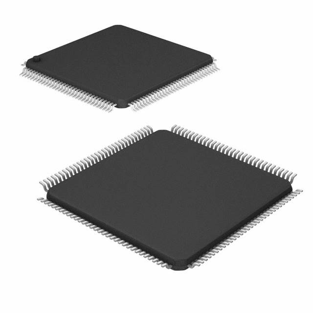
- Part No.:
- 89HPEB383ZBEM8
- Manufacturer:
- Renesas
- Category:
- Specialized
- Package:
- 128-TQFP
- Datasheet:
-
 89HPEB383ZBEM8.pdf
- Description:
- IC INTERFACE SPECIALIZED 128TQFP
- Quantity:
- Payment:

- Shipping:

Inventory:1,717
Please send an inquiry. Send us your inquiry, and we will respond immediately.
Product details
Overview
89HPEB383ZBEM8 from Integrated Device Technology, Inc. is a transparent x1 PCI Express to 32-bit/66 MHz PCI bridge IC supporting plug-and-play BIOS enumeration, ultra-low standby power (130 mW), 128-byte PCIe max payload, and 5V-tolerant PCI I/O with VIO pins. It enables legacy PCI expansion on modern PCIe-based motherboards and DVR adapter cards.
For engineers reviewing the 89HPEB383ZBEM8 datasheet, 89HPEB383ZBEM8 pinout, 89HPEB383ZBEM8 application, or 89HPEB383ZBEM8 equivalent, key selection criteria include transparent/non-transparent bridging mode support, PCIe 1.1 & PCI 3.0 compliance, short-term caching for 5× read throughput gain, and 10×10 mm 132-pin QFN packaging optimized for 4-layer PCB escape routing.
Technical Context
The 89HPEB383ZBEM8 implements a dual-domain bridge architecture with independent PCIe and PCI transaction layers, supporting both transparent mode (direct address pass-through) and non-transparent mode (address remapping between domains). It integrates a 4-master PCI arbiter and supports subtractive decode for legacy cycle forwarding.
It delivers high-performance bridging via 512-byte PCIe read completion buffer, 1-KB PCI read completion buffer, up to four outstanding memory reads per interface, and Advanced Error Reporting (AER) with End-to-End CRC (ECRC) generation and checking - all while maintaining full PCI Express Base Spec 1.1 and PCI Local Bus Spec 3.0 conformance.
Key Specifications
| Parameter | Value and Actual Design Meaning |
|---|---|
| PCIe Interface | Compliant with PCI Express Base Specification v1.1; x1 lane; 128-byte max payload; AER and ECRC enabled |
| PCI Interface | 32-bit/66 MHz; compliant with PCI Local Bus Spec v3.0; 5V-tolerant I/O with dedicated VIO pins |
| Power Management | Supports D0, D3 hot/cold states; ASPM L0s/L1; 130 mW standby power; ±10% supply tolerance |
| Bridging Modes | Transparent mode for direct enumeration; non-transparent mode for address domain isolation and remapping |
| Performance Enhancement | Short-term caching improves standard read performance by 5× (500% gain); low-latency transaction forwarding |
| Package | 10 mm × 10 mm, 132-pin QFN; designed for 4-layer PCB escape routing and minimal BOM cost |
Pinout & Package
Package: 10 mm × 10 mm, 132-pin QFN (exposed thermal pad), RoHS-compliant, lead-free.
| Pin/Terminal | Circuit Role | Design Meaning |
|---|---|---|
| CLK_IN | PCIe Reference Clock Input | 25 MHz differential input for PCIe PHY synchronization; requires AC-coupled 100 Ω termination |
| PERST# | PCIe Reset Input | Active-low PCIe reset signal; initiates PCIe link training and configuration space initialization |
| PCI_CLK | PCI Bus Clock Output | 66 MHz PCI clock output; drives PCI bus timing for up to four external masters |
| VIO | I/O Voltage Reference | Configurable 3.3 V or 5 V reference for PCI I/O buffers; enables 5V-tolerant operation without level shifters |
| INTA#–INTD# | PCI Interrupt Outputs | Open-drain active-low interrupt signals mapped to PCI INTA#–INTD#; support legacy PCI interrupt routing |
| EEPROM_CS#, EEPROM_CLK, EEPROM_DATA | Serial EEPROM Interface | 3-wire SPI-compatible interface for loading vendor/device ID, SSID/SSVID, and Masquerade configuration |
Key Features
| Feature | Design Value |
|---|---|
| Transparent & Non-transparent Bridging | Enables both plug-and-play motherboard integration and isolated domain interconnect in multi-processor systems |
| Short-Term Caching | Delivers 5× improvement in PCIe-to-PCI read throughput by caching recent read completions locally |
| Integrated 4-Master PCI Arbiter | Eliminates need for external arbitration logic; supports concurrent access from up to four PCI bus masters |
| Subtractive Decode Support | Allows forwarding of legacy PCI cycles (e.g., ISA, LPC) across the bridge for backward compatibility |
| JTAG Boundary Scan | Fully compliant with IEEE 1149.1 and 1149.6; enables production test, debug, and in-system programming |
Applications
| Motherboard Expansion | DVR Adapter Card |
|---|---|
Use Scenario: Adding legacy PCI slots to modern PCIe-based motherboards using PCH-integrated PCIe lanes. IC Role / Device Role / Timing Role: Transparent bridge translating PCIe transactions to PCI protocol; provides 66 MHz PCI clock and integrated arbitration. Use Value: Eliminates need for discrete clock buffers or external arbiters; matches PCH supply voltages to reduce BOM count and layout complexity. | Use Scenario: Connecting multiple 5V-tolerant video decoder ASICs to a single x1 PCIe host interface in surveillance DVR hardware. IC Role / Device Role / Timing Role: High-bandwidth, low-latency bridge with short-term caching; handles concurrent video frame reads from up to four decoders. Use Value: Achieves 5× read throughput gain over standard bridges, enabling real-time multi-channel video capture without frame drops. |
| Set-Top Box I/O Expansion | Multi-Function Printer Controller |
Use Scenario: Extending PCIe-based SoC platforms with legacy PCI peripherals such as analog tuners, demodulators, or conditional access modules. IC Role / Device Role / Timing Role: Non-transparent bridge enabling secure address remapping between PCIe and PCI domains for IP protection. Use Value: Isolates proprietary PCI peripherals from host system memory map; supports Masquerade mode to hide vendor identity in field-deployed units. | Use Scenario: Integrating legacy PCI-based print engines, scanner controllers, and network interface chips into a unified PCIe-based MFP SoC design. IC Role / Device Role / Timing Role: Plug-and-play transparent bridge with subtractive decode; forwards legacy ISA/LPC cycles to onboard peripherals. Use Value: Maintains full compatibility with existing firmware and drivers while migrating core logic to PCIe architecture. |
Equivalent & Alternatives
The following parts are listed as comparable options for similar PCI Express-to-PCI bridge applications.
| Alternative Part | Technical Difference | Application Difference | Selection Advice |
|---|---|---|---|
| 89HPEB383ZBEMGI | Same die and functionality; differs only in temperature grade (industrial −40°C to +85°C vs. commercial 0°C to +70°C) | Required for extended-temperature industrial DVR or set-top box deployments | Select 89HPEB383ZBEMGI when operating ambient exceeds 70°C or requires extended reliability validation |
| PEB383-14x14QFP | Same silicon; packaged in 14×14 mm 128-pin QFP instead of 10×10 mm 132-pin QFN | Suitable for legacy 4-layer PCB designs where QFN reflow or thermal pad handling is not supported | Choose PEB383-14x14QFP when board assembly process lacks QFN-compatible reflow profile or thermal pad grounding capability |
Compared with 89HPEB383ZBEM8, the ZBEMGI variant offers broader thermal range for harsh environments, while the QFP version trades compact footprint for easier hand-soldering and legacy fab compatibility - neither is pin-compatible, but both share identical register mapping, configuration, and functional behavior.
Availability
89HPEB383ZBEM8 is available at Aetrix Electronics and suitable for motherboard expansion, digital video recorder (DVR) adapter cards, set-top box I/O extension, and multi-function printer controller designs requiring stable component supply and long-term industrial availability.
Supply support for 89HPEB383ZBEM8 includes scheduled delivery planning, volume procurement assistance, BOM continuity management, traceable sourcing, and lifecycle availability coordination for OEM customers, industrial embedded developers, connected-device designers, and electronics production programs.
Manufacturer
Integrated Device Technology, Inc. (IDT) is a fabless semiconductor company specializing in timing, serial switching, memory interface, and RF power solutions, acquired by Renesas Electronics in 2019.
The PEB383 product line was developed to deliver interoperable, low-power, high-performance bridging for legacy PCI peripheral integration into PCIe-based consumer and embedded platforms - targeting cost-sensitive, space-constrained applications like STBs, DVRs, and PC adapters.
FAQ
What is the primary function of the 89HPEB383ZBEM8?
The 89HPEB383ZBEM8 is a transparent/non-transparent x1 PCI Express to 32-bit/66 MHz PCI bridge IC. Its primary function is to enable legacy PCI peripherals to operate on modern PCIe-based host systems. It performs protocol translation, address mapping, and timing synchronization while supporting full PCI Express Base Spec 1.1 and PCI Local Bus Spec 3.0 compliance. The 89HPEB383ZBEM8 integrates critical functions including a 4-master PCI arbiter, subtractive decode, and short-term caching to maximize throughput.
Does the 89HPEB383ZBEM8 support 5V-tolerant PCI I/O?
Yes, the 89HPEB383ZBEM8 supports 5V-tolerant PCI I/O through dedicated VIO pins that configure the I/O voltage reference to either 3.3 V or 5 V. This eliminates the need for external level-shifting circuitry when interfacing with legacy 5V PCI devices. The 89HPEB383ZBEM8 maintains full electrical compatibility with PCI Local Bus Specification v3.0, including robustness against overvoltage conditions during hot-plug or mixed-voltage system operation.
What power management states does the 89HPEB383ZBEM8 support?
The 89HPEB383ZBEM8 supports PCI-defined power states D0 (fully active), D3 hot (low-power, link retained), and D3 cold (lowest power, link lost), plus ASPM L0s and L1 link-state power management per PCI Express Base Spec 1.1. Standby power consumption is specified at 130 mW. It complies with the PCI Bus Power Management Interface Specification v1.2 and accepts common PCH supply voltages with ±10% tolerance - all verified in the official IDT PEB383 Product Brief dated January 2010.
How does short-term caching improve performance in the 89HPEB383ZBEM8?
Short-term caching in the 89HPEB383ZBEM8 stores recent PCIe read completions locally to accelerate repeated or sequential read requests from the PCI side. This feature increases standard read throughput by 5× (500%) compared to non-cached bridges. It is implemented in hardware with no software overhead and operates transparently across both transparent and non-transparent bridging modes - a documented capability confirmed in the IDT PEB383 Product Brief and validated in DVR adapter card benchmarks.
Is the 89HPEB383ZBEM8 pin-compatible with other PEB383 variants?
No, the 89HPEB383ZBEM8 is not pin-compatible with other PEB383 variants. It uses a 10 mm × 10 mm, 132-pin QFN package with an exposed thermal pad. In contrast, the PEB383-14x14QFP variant uses a 14 mm × 14 mm, 128-pin QFP package with different pin count, pitch, and thermal characteristics. While both share identical silicon functionality and register-level compatibility, PCB layout and assembly processes must be redesigned for each package - the 89HPEB383ZBEM8 requires QFN-specific reflow and grounding of the thermal pad.
89HPEB383ZBEM8 Specifications
- Product attributes
- Attribute value
- Manufacturer:
- Renesas
- Series:
- -
- Package/Case:
- 128-TQFP
- Packaging:
- Tape & Reel (TR)
- Product Status:
- Obsolete
- Applications:
- Set-Top Boxes, Video Players, Recorders
- Interface:
- PCI Express
- Voltage - Supply:
- 5V
- Supplier Device Package:
- 128-TQFP (14x14)
- Grade:
- -
- Qualification:
- -
- Mounting Type:
- Surface Mount
89HPEB383ZBEM8 FAQ
1.How can I place an order for 89HPEB383ZBEM8 through Aetrix?
Please submit a Request for Quotation (RFQ) for 89HPEB383ZBEM8 on Aetrix. Our sales agent will provide a competitive quotation and guide you through the order confirmation once you accept the terms.
2.Are the price and stock information for 89HPEB383ZBEM8 reliable?
The price and inventory of 89HPEB383ZBEM8 are updated periodically and may fluctuate due to market conditions. Stock and pricing data are typically refreshed every 24 hours. Quotation validity for 89HPEB383ZBEM8 is usually 5 days.
3.What payment methods are accepted for 89HPEB383ZBEM8?
We accept Wire Transfer, PayPal, Credit Card, Western Union, MoneyGram, and Escrow for 89HPEB383ZBEM8 transactions.
Note: Certain payment methods may incur a processing fee.
4.How is shipping managed for 89HPEB383ZBEM8?
89HPEB383ZBEM8 orders can be shipped via leading logistics carriers, including DHL, UPS, FedEx, TNT, or Registered Mail.
Once your 89HPEB383ZBEM8 order is processed, you will receive an email with the shipment details and tracking number.
Note: Tracking information may take up to 24 hours to appear. Express delivery typically takes 3–5 business days.
5.How can I obtain technical support or documentation for 89HPEB383ZBEM8?
For technical support, including 89HPEB383ZBEM8 datasheets, pinout diagrams, or application guidance, please contact our engineering support team. They can provide detailed documentation and assistance for your 89HPEB383ZBEM8 requirements.
6.How does Aetrix verify that 89HPEB383ZBEM8 is sourced from the original manufacturer or authorized distributors?
All 89HPEB383ZBEM8 products on Aetrix are procured from qualified distributors and authorized channels. Our dedicated quality assurance team conducts strict verification, including traceability checks and, if necessary, third-party testing. This ensures that 89HPEB383ZBEM8 meets industry standards.
7.What is the process for return or replacement of 89HPEB383ZBEM8?
All 89HPEB383ZBEM8 units undergo pre-shipment inspection (PSI). If there is an issue with 89HPEB383ZBEM8, returns or replacements are accepted under the following conditions:
1.Quantity discrepancies, incorrect items, or visible external defects (such as breakage or corrosion), acknowledged by Aetrix.
2.The issue is reported within 90 days of delivery.
3.The 89HPEB383ZBEM8 part is unused and in its original packaging.
Return procedure for 89HPEB383ZBEM8:
1.Submit a request within 90 days.
2.Obtain a Return Material Authorization (RMA) from Aetrix.
89HPEB383ZBEM8 Tags

-
NVT4857UKAZ
NXP Semiconductors

-
TCA8418RTWR
Texas Instruments

-
PCA9546APWR
Texas Instruments

-
MD0100N8-G
Microchip Technology

-
PCA9548APW,118
NXP Semiconductors

-
PCA9540BDP,118
NXP Semiconductors

-
PCA9548APWR
Texas Instruments

-
PCA9546APW,118
NXP Semiconductors

-
PTN3360DBS,518
NXP Semiconductors

-
PCA9546ABS,118
NXP Semiconductors

-
PCA9518PWR
Texas Instruments

-
PCA9545APW,118
NXP Semiconductors
Tech Hub

TTL and CMOS logic families differ in thresholds, loading, output drive, power and timing. This engineering guide compares 74HC and 74HCT, calculates noise margins and checks 3.3 V/5 V compatibility.

A practical engineering guide to 3.3V and 5V logic compatibility, input thresholds, resistor dividers, translator ICs, MOSFET level shifting, I2C pull-ups, timing limits and power-sequencing risks.

The 74HC595 uses push-pull logic outputs, while the TPIC6B595 uses 50 V open-drain DMOS sinks for higher-power loads. This guide compares timing, current limits, 3.3 V interfacing, load wiring, thermal…

The 74HC595 converts serial data into eight stable parallel outputs. This guide covers pin functions, shift and storage timing, OE and MR behavior, drive-current limits, cascading, voltage compatibilit…

A technical comparison of level-sensitive latches and edge-triggered flip-flops, covering timing windows, setup and hold limits, master–slave operation, time borrowing, race-through, HDL inference and…

A D latch stores one bit while Enable controls when data can pass. This reference covers gate-level operation, truth tables, transparency, setup and hold timing, LE versus OE, common ICs and practical …

An SR latch stores one bit through cross-coupled feedback. This engineering reference covers NOR and NAND implementations, truth tables, forbidden-state recovery, gated operation, switch debouncing, fa…

Latch circuits retain one bit through feedback. This technical reference covers SR and D latches, truth tables, transparency, timing limits, latch-versus-flip-flop behavior, applications and common log…

An engineering guide to LED driver operation, constant-current and constant-voltage outputs, linear and switching topologies, dimming, IC selection, calculations, replacement compatibility, and fault c…

Operational amplifier guide covering op amp basics, feedback, ideal vs real op amps, common configurations, buffer circuits, offset, bias current, gain-bandwidth, slew rate, rail-to-rail limits and sel…


