
 My Inquiry
 My Account


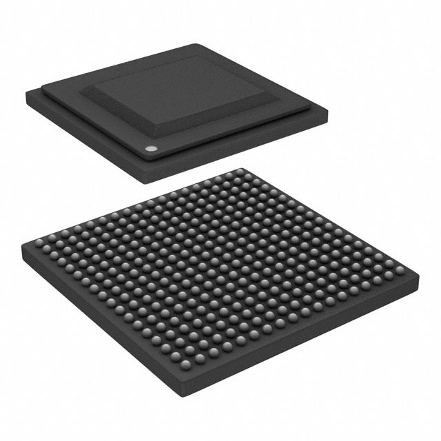
Renesas 89HPES12N3A2ZCBC8
- Part No.:
- 89HPES12N3A2ZCBC8
- Manufacturer:
- Renesas
- Category:
- Specialized
- Package:
- 324-BGA
- Datasheet:
-
 89HPES12N3A2ZCBC8.pdf
- Description:
- IC INTFACE SPECIALIZED 324CABGA
- Quantity:
- Payment:

- Shipping:

Inventory:4,376
Please send an inquiry. Send us your inquiry, and we will respond immediately.
Product details
Overview
89HPES12N3A2ZCBC8 from IDT is a 12-lane, 3-port PCI Express 1.1 switch IC with x4 upstream and two x4 downstream ports, 2.5 Gbps per lane, cut-through architecture, and integrated 8B/10B SerDes - deployed in server I/O expansion, storage interconnects, and communications chassis.
For engineers reviewing the 89HPES12N3A2ZCBC8 datasheet, 89HPES12N3A2ZCBC8 pinout, 89HPES12N3A2ZCBC8 application, or 89HPES12N3A2ZCBC8 equivalent, key selection considerations include PCIe 1.1 compliance, configurable link widths (x1/x2/x4), SMBus-configurable operation, Hot-Plug support via external expander, and thermal performance in 19×19 mm BGA packages.
Technical Context
The 89HPES12N3A2ZCBC8 implements a layered PCI Express switch core with separate Transaction, Data Link, and Physical layers compliant with Base Specification Revision 1.1. It supports eight traffic classes and one virtual channel, with internal frame buffering and route table arbitration for deterministic latency.
Its dual SMBus interface enables both slave-mode register access and master-mode configuration loading from serial EEPROM; GPIO[0–7] provide flexible I/O control including port reset outputs (P2RSTN/P4RSTN) and Hot-Plug interrupt inputs (IOEXPINTN0/IOEXPINTN2).
Key Specifications
| Parameter | Value and Actual Design Meaning |
|---|---|
| PCIe Version | Compliant with PCI Express Base Specification Revision 1.1 - ensures interoperability with Gen1 root complexes and endpoints. |
| Lane Count & Speed | 12 lanes total, each operating at 2.5 Gbps bidirectional - delivers up to 4 GB/s aggregate bandwidth across three ports. |
| Port Configuration | 1 upstream port (configurable up to x4) + 2 downstream ports (each configurable up to x4) - enables flexible topologies like fan-out or daisy-chain. |
| Switch Architecture | Cut-through forwarding with low-latency path - reduces packet delay vs store-and-forward, critical for real-time I/O consolidation. |
| Max Payload Size | Supports up to 2048 bytes - aligns with standard PCIe MTU for efficient large-block transfers in storage and networking. |
| Power Management | Supports D0, D3hot, D3cold states per PCI-PM 1.1 - enables system-level power gating and thermal-aware runtime control. |
| Reference Clock | Accepts 100 MHz or 125 MHz differential input (selected by REFCLKM) - matches common motherboard clock sources without external synthesis. |
| Package | 324-ball BGA, 19×19 mm, 1.0 mm ball pitch - compatible with standard high-density PCB assembly processes. |
Pinout & Package
Package: 324-ball BGA, 19 mm × 19 mm, 1.0 mm ball pitch, RoHS-compliant.
| Pin/Terminal | Circuit Role | Design Meaning |
|---|---|---|
| PE0RP[3:0]/PE0RN[3:0] | Upstream RX differential pair | Receives PCIe 2.5 Gbps serial data from root complex; CML input with AC coupling required. |
| PE0TP[3:0]/PE0TN[3:0] | Upstream TX differential pair | Transmits PCIe 2.5 Gbps serial data to root complex; includes de-emphasis and DC common-mode control. |
| PE2RP[3:0]/PE2RN[3:0], PE4RP[3:0]/PE4RN[3:0] | Downstream RX pairs (Port 2 & Port 4) | Receive from endpoint devices; support lane reversal and polarity inversion automatically. |
| PE2TP[3:0]/PE2TN[3:0], PE4TP[3:0]/PE4TN[3:0] | Downstream TX pairs (Port 2 & Port 4) | Drive PCIe endpoints; integrated SerDes eliminates need for external transceivers. |
| SSMBCLK/SSMBDAT, SSMBADDR[5,3:1] | Slave SMBus interface | Enables full read/write access to all internal configuration registers by host processor or BMC. |
| MSMBCLK/MSMBDAT, MSMBADDR[4:1] | Master SMBus interface | Loads default configuration from external EEPROM post-reset; interfaces with Hot-Plug expanders. |
| GPIO[0], GPIO[1] | Configurable I/O with alternate functions | GPIO[0] = P2RSTN (Port 2 reset output); GPIO[1] = P4RSTN (Port 4 reset output) - simplifies endpoint reset sequencing. |
| GPIO[2], GPIO[4] | Interrupt-capable I/O | GPIO[2] = IOEXPINTN0, GPIO[4] = IOEXPINTN2 - receive Hot-Plug status changes from I/O expander. |
| PERSTN, RSTHALT | Fundamental reset control | PERSTN initiates full PCIe reset; RSTHALT holds device in reset while allowing SMBus register access for debug/configuration. |
| JTAG_TCK/TDI/TDO/TMS/TRST_N | IEEE 1149.1 boundary scan | Enables production test, in-system debugging, and firmware validation without physical probe access. |
Key Features
| Feature | Design Value |
|---|---|
| No external components required | On-chip SerDes, memory buffers, and logic eliminate discrete transceivers, FIFOs, and configuration PROMs - reduces BOM count and board area. |
| Automatic link negotiation | Each port independently negotiates x1/x2/x4 width and handles lane reversal/polarity inversion - simplifies layout and improves field reliability. |
| End-to-end parity protection | Internal parity on all TLPs ensures data integrity even in systems lacking ECRC - enhances RAS for mission-critical servers and storage. |
| Hot-Plug I/O expander interface | SMBus master interface directly controls standard PC/server Hot-Plug expanders (e.g., TI TPS2359) - avoids custom ASIC glue logic. |
| Flexible power management | Unused SerDes blocks are disabled; D3cold entry reduces leakage - achieves typical 1.96 W power at 35% link utilization. |
| Eight configurable GPIOs | Each pin supports input/output mode, interrupt capability, and documented alternate functions (e.g., P2RSTN, IOEXPINTN0) - enables system-specific control without external logic. |
Applications
| Server I/O Expansion | Enterprise Storage Interconnect |
|---|---|
Use Scenario: Adding multiple PCIe slots to a 1U/2U rack server via a single upstream link to the CPU socket. IC Role / Device Role / Timing Role: PCI Express switch providing non-blocking connectivity between CPU root port and four NVMe SSDs or dual-port 10GbE NICs. Use Value: Enables cost-effective I/O scaling without requiring additional root complexes or chipset upgrades - maintains Gen1 compatibility across legacy infrastructure. | Use Scenario: Building a modular JBOD enclosure where backplane lanes fan out to 12 SAS/SATA drives via PCIe-to-SAS bridges. IC Role / Device Role / Timing Role: Central switching hub aggregating PCIe traffic from host controller to distributed bridge chips, supporting hot-swap drive bays. Use Value: Delivers deterministic latency (<150 ns cut-through) and ECRC-protected packet routing - essential for RAID rebuild consistency and error containment. |
| Communications Chassis Backplane | Industrial Embedded Computing |
Use Scenario: High-density telecom blade server with shared PCIe fabric across compute, packet processing, and FPGA acceleration modules. IC Role / Device Role / Timing Role: Low-latency interconnect enabling peer-to-peer DMA between FPGA-based line cards and x86 control plane. Use Value: Eight traffic classes allow strict QoS prioritization of control-plane vs data-plane traffic - meets sub-millisecond jitter requirements for real-time packet forwarding. | Use Scenario: Ruggedized medical imaging system integrating GPU-accelerated image reconstruction with PCIe-connected CT detector interface cards. IC Role / Device Role / Timing Role: Reliable I/O concentrator handling simultaneous high-bandwidth streams from multiple sensor modules under extended temperature range (-40°C to +85°C). Use Value: Industrial-grade thermal design (θJA = 21.8°C/W, no heatsink required at 1 m/s airflow) ensures continuous operation in sealed enclosures. |
Equivalent & Alternatives
The following parts are listed as comparable options for similar PCI Express switch applications.
| Alternative Part | Technical Difference | Application Difference | Selection Advice |
|---|---|---|---|
| 89HPES12T3AG2ZBBC | Same 12-lane, 3-port architecture but with industrial temperature grade (-40°C to +85°C) and enhanced ESD rating (±8 kV HBM). | Required for deployments in harsh environments (e.g., base station cabinets, factory automation) where commercial-grade thermal margin is insufficient. | Select when ambient exceeds 70°C or system-level ESD immunity must exceed 4 kV. |
| 89HPES8T3AG2ZBBC | 8-lane variant with identical feature set, package, and pinout - reduced lane count lowers power (1.44 W typical) and cost. | Suitable for space-constrained edge servers or embedded systems where full 12-lane bandwidth is unnecessary. | Choose when application uses only two downstream endpoints (e.g., one GPU + one NVMe) and board area/power budget are constrained. |
Compared with 89HPES12N3A2ZCBC8, the 89HPES12T3AG2ZBBC offers extended temperature operation and higher ESD robustness at identical functionality, while the 89HPES8T3AG2ZBBC trades 4 lanes for lower power and cost - enabling tiered product families without redesigning PCB layout or firmware.
Availability
89HPES12N3A2ZCBC8 is available at Aetrix Electronics and suitable for server I/O expansion, enterprise storage interconnect, and communications chassis backplane applications requiring stable component supply across multi-year production cycles.
Supply support for 89HPES12N3A2ZCBC8 includes scheduled delivery planning, volume procurement assistance, BOM continuity management, traceable sourcing, and lifecycle availability coordination for OEM customers, industrial embedded developers, connected-device designers, and electronics production programs.
Manufacturer
IDT (Integrated Device Technology, Inc.) is a fabless semiconductor company specializing in timing, memory interface, RF, and high-performance interconnect solutions, acquired by Renesas Electronics in 2019.
The PRECISE™ family - including the 89HPES12N3A2ZCBC8 - was designed specifically for high-reliability, low-latency PCI Express switching in data center and telecom infrastructure, emphasizing RAS features, thermal efficiency, and seamless integration with legacy BIOS and OS drivers.
FAQ
What PCIe specification revision does the 89HPES12N3A2ZCBC8 implement?
The 89HPES12N3A2ZCBC8 implements PCI Express Base Specification Revision 1.1. It supports 2.5 Gbps per lane, 8B/10B encoding, and all mandatory features including Advanced Error Reporting and ECRC. It does not support PCIe 2.0 or later revisions, and its maximum payload size is limited to 2048 bytes per TLP. The 89HPES12N3A2ZCBC8 remains fully interoperable with Gen1 root complexes and endpoints in production server and storage platforms.
Does the 89HPES12N3A2ZCBC8 require external SerDes or transceivers?
No, the 89HPES12N3A2ZCBC8 integrates twelve 2.5 Gbps embedded SerDes with full 8B/10B encoder/decoder functionality - eliminating the need for external transceivers. All PCIe electrical signaling (TX/RX differential pairs, reference clock interface, and termination) is handled internally. This integration reduces bill-of-materials cost, PCB layer count, and layout complexity compared to discrete PHY+switch solutions.
How is Hot-Plug functionality implemented on the 89HPES12N3A2ZCBC8?
The 89HPES12N3A2ZCBC8 implements Hot-Plug via its master SMBus interface, which communicates with standard external I/O expanders (e.g., TI TPS2359) rather than using dedicated Hot-Plug pins. Upon detecting a slot insertion/removal event, the expander asserts an interrupt on GPIO[2] or GPIO[4], and the 89HPES12N3A2ZCBC8 responds by issuing SMBus commands to update power and presence status. This architecture reuses existing motherboard infrastructure and avoids adding dedicated Hot-Plug ASIC logic.
What are the power-up sequencing requirements for the 89HPES12N3A2ZCBC8?
The 89HPES12N3A2ZCBC8 requires strict power-up sequencing: (1) VDDIO (3.3 V) first, (2) then VDDCORE, VDDPE, and VDDAPE (all 1.0 V), and (3) finally VTTPE (1.5 V). Each rail must ramp and stabilize before the next is applied to prevent latch-up. Power-down must follow the reverse order. Deviation from this sequence risks functional failure or permanent damage. The 89HPES12N3A2ZCBC8 does not include internal power sequencing circuitry - external supervisors or sequencers are required.
Can the 89HPES12N3A2ZCBC8 operate in store-and-forward mode?
Yes, the 89HPES12N3A2ZCBC8 supports both cut-through and store-and-forward switching modes. Cut-through is the default and lowest-latency mode, forwarding packets as soon as header routing information is available. Store-and-forward mode buffers entire packets before forwarding - used when end-to-end CRC checking or deep packet inspection is required. Mode selection is controlled via configuration registers accessible through the slave SMBus interface or serial EEPROM.
89HPES12N3A2ZCBC8 Specifications
- Product attributes
- Attribute value
- Manufacturer:
- Renesas
- Series:
- PRECISE™
- Package/Case:
- 324-BGA
- Packaging:
- Tape & Reel (TR)
- Product Status:
- Obsolete
- Applications:
- Switch Interfacing
- Interface:
- PCI Express
- Voltage - Supply:
- 3.3V
- Supplier Device Package:
- 324-CABGA (19x19)
- Grade:
- -
- Qualification:
- -
- Mounting Type:
- Surface Mount
89HPES12N3A2ZCBC8 FAQ
1.How can I place an order for 89HPES12N3A2ZCBC8 through Aetrix?
Please submit a Request for Quotation (RFQ) for 89HPES12N3A2ZCBC8 on Aetrix. Our sales agent will provide a competitive quotation and guide you through the order confirmation once you accept the terms.
2.Are the price and stock information for 89HPES12N3A2ZCBC8 reliable?
The price and inventory of 89HPES12N3A2ZCBC8 are updated periodically and may fluctuate due to market conditions. Stock and pricing data are typically refreshed every 24 hours. Quotation validity for 89HPES12N3A2ZCBC8 is usually 5 days.
3.What payment methods are accepted for 89HPES12N3A2ZCBC8?
We accept Wire Transfer, PayPal, Credit Card, Western Union, MoneyGram, and Escrow for 89HPES12N3A2ZCBC8 transactions.
Note: Certain payment methods may incur a processing fee.
4.How is shipping managed for 89HPES12N3A2ZCBC8?
89HPES12N3A2ZCBC8 orders can be shipped via leading logistics carriers, including DHL, UPS, FedEx, TNT, or Registered Mail.
Once your 89HPES12N3A2ZCBC8 order is processed, you will receive an email with the shipment details and tracking number.
Note: Tracking information may take up to 24 hours to appear. Express delivery typically takes 3–5 business days.
5.How can I obtain technical support or documentation for 89HPES12N3A2ZCBC8?
For technical support, including 89HPES12N3A2ZCBC8 datasheets, pinout diagrams, or application guidance, please contact our engineering support team. They can provide detailed documentation and assistance for your 89HPES12N3A2ZCBC8 requirements.
6.How does Aetrix verify that 89HPES12N3A2ZCBC8 is sourced from the original manufacturer or authorized distributors?
All 89HPES12N3A2ZCBC8 products on Aetrix are procured from qualified distributors and authorized channels. Our dedicated quality assurance team conducts strict verification, including traceability checks and, if necessary, third-party testing. This ensures that 89HPES12N3A2ZCBC8 meets industry standards.
7.What is the process for return or replacement of 89HPES12N3A2ZCBC8?
All 89HPES12N3A2ZCBC8 units undergo pre-shipment inspection (PSI). If there is an issue with 89HPES12N3A2ZCBC8, returns or replacements are accepted under the following conditions:
1.Quantity discrepancies, incorrect items, or visible external defects (such as breakage or corrosion), acknowledged by Aetrix.
2.The issue is reported within 90 days of delivery.
3.The 89HPES12N3A2ZCBC8 part is unused and in its original packaging.
Return procedure for 89HPES12N3A2ZCBC8:
1.Submit a request within 90 days.
2.Obtain a Return Material Authorization (RMA) from Aetrix.
89HPES12N3A2ZCBC8 Tags

-
NVT4857UKAZ
NXP Semiconductors

-
TCA8418RTWR
Texas Instruments

-
PCA9546APWR
Texas Instruments

-
MD0100N8-G
Microchip Technology

-
PCA9548APW,118
NXP Semiconductors

-
PCA9540BDP,118
NXP Semiconductors

-
PCA9548APWR
Texas Instruments

-
PCA9546APW,118
NXP Semiconductors

-
PTN3360DBS,518
NXP Semiconductors

-
PCA9546ABS,118
NXP Semiconductors

-
PCA9518PWR
Texas Instruments

-
PCA9545APW,118
NXP Semiconductors
Tech Hub

TTL and CMOS logic families differ in thresholds, loading, output drive, power and timing. This engineering guide compares 74HC and 74HCT, calculates noise margins and checks 3.3 V/5 V compatibility.

A practical engineering guide to 3.3V and 5V logic compatibility, input thresholds, resistor dividers, translator ICs, MOSFET level shifting, I2C pull-ups, timing limits and power-sequencing risks.

The 74HC595 uses push-pull logic outputs, while the TPIC6B595 uses 50 V open-drain DMOS sinks for higher-power loads. This guide compares timing, current limits, 3.3 V interfacing, load wiring, thermal…

The 74HC595 converts serial data into eight stable parallel outputs. This guide covers pin functions, shift and storage timing, OE and MR behavior, drive-current limits, cascading, voltage compatibilit…

A technical comparison of level-sensitive latches and edge-triggered flip-flops, covering timing windows, setup and hold limits, master–slave operation, time borrowing, race-through, HDL inference and…

A D latch stores one bit while Enable controls when data can pass. This reference covers gate-level operation, truth tables, transparency, setup and hold timing, LE versus OE, common ICs and practical …

An SR latch stores one bit through cross-coupled feedback. This engineering reference covers NOR and NAND implementations, truth tables, forbidden-state recovery, gated operation, switch debouncing, fa…

Latch circuits retain one bit through feedback. This technical reference covers SR and D latches, truth tables, transparency, timing limits, latch-versus-flip-flop behavior, applications and common log…

An engineering guide to LED driver operation, constant-current and constant-voltage outputs, linear and switching topologies, dimming, IC selection, calculations, replacement compatibility, and fault c…

Operational amplifier guide covering op amp basics, feedback, ideal vs real op amps, common configurations, buffer circuits, offset, bias current, gain-bandwidth, slew rate, rail-to-rail limits and sel…


