
 My Inquiry
 My Account


Renesas 89HT0808PYAABI
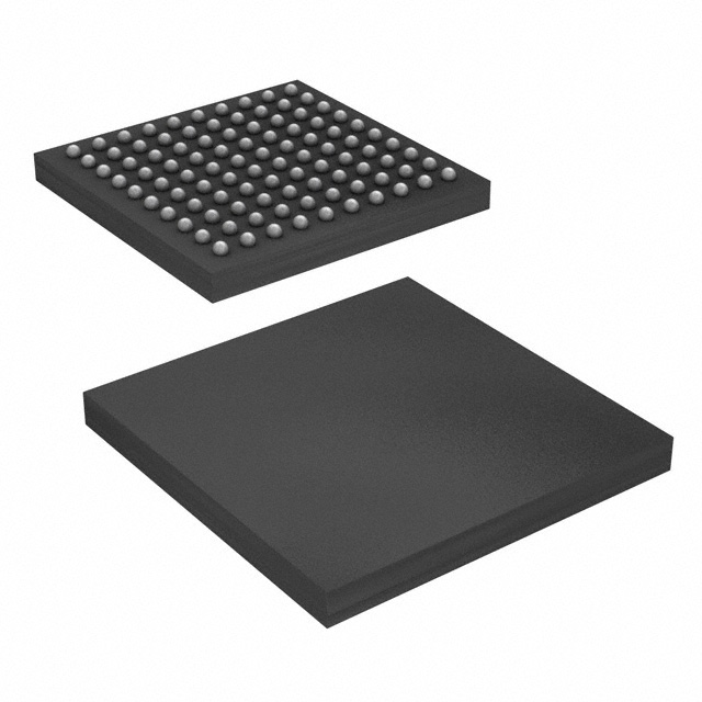
- Part No.:
- 89HT0808PYAABI
- Manufacturer:
- Renesas
- Category:
- Specialized
- Package:
- 100-LFBGA
- Datasheet:
-
 89HT0808PYAABI.pdf
- Description:
- IC INTFACE SPECIALIZED 100FPBGA
- Quantity:
- Payment:

- Shipping:

Inventory:3,190
Please send an inquiry. Send us your inquiry, and we will respond immediately.
Product details
Overview
89HT0808PYAABI from Integrated Device Technology is an 8-channel PCIe® 3.0 signal retimer IC that conditions high-speed serial links by eliminating random and deterministic jitter, compensating for PCB trace/cable attenuation, and resetting the jitter budget. It supports 8.0 Gbps (PCIe Gen 3), 5.0 Gbps (Gen 2), and 2.5 Gbps (Gen 1) per lane across up to four full x1/x2/x4 PCIe lanes in a 9×9 mm, 100-ball BGA package.
For engineers reviewing the 89HT0808PYAABI datasheet, 89HT0808PYAABI pinout, 89HT0808PYAABI application, or 89HT0808PYAABI equivalent, key selection considerations include per-lane CTLE+5-tap DFE equalization, I²C-configurable de-emphasis (up to 8 dB), L0s/L1 ASPM power management, PCIe Base Spec 3.0/2.1 compliance, and integrated SERDES test modes with IEEE 1149.1/1149.6 JTAG support.
Technical Context
The 89HT0808PYAABI implements a full PCIe Gen 3 retiming architecture with independent Rx/Tx SERDES per channel, including multi-stage CTLE and 5-tap DFE for deterministic ISI compensation and adaptive clock recovery via fast-acquisition PLL. It supports both common-clock and non-common-clock PCIe topologies with SSCLK compatibility.
Its physical layer includes end-to-end data path parity protection, on-chip eye generation for diagnostics, and per-lane configuration of drive strength, receive equalization, and transmit de-emphasis - all accessible via dedicated master/slave I²C interfaces or JTAG for debug and EEPROM programming.
Key Specifications
| Parameter | Value and Actual Design Meaning |
|---|---|
| Data Rate | Supports 2.5 Gbps (Gen 1), 5.0 Gbps (Gen 2), and 8.0 Gbps (Gen 3) per lane - enables backward-compatible deployment across PCIe generations. |
| Channels | 8 differential lanes configurable as up to four x2 or two x4 PCIe links - provides flexible topology mapping for server backplanes and storage interconnects. |
| Equalization | CTLE + 5-tap DFE per receiver - actively compensates frequency-dependent loss and inter-symbol interference on FR4 traces or passive cables. |
| Transmit De-emphasis | Up to 8 dB programmable de-emphasis - meets PCIe Gen 3 transmitter mask requirements for long-reach backplane applications. |
| Power Management | Supports L0s and L1 ASPM states with automatic low-power shutdown of unused SerDes lanes - reduces dynamic power in partial-link configurations. |
| Clock Input | 100 MHz differential reference clock input with spread-spectrum clocking (SSCLK) support - ensures timing alignment in common-clock PCIe systems. |
| Interface | Dedicated I²C master and slave ports - enables external EEPROM boot configuration and real-time CSR access without host CPU intervention. |
Pinout & Package
Package: 100-ball BGA, 9 mm × 9 mm, 0.8 mm ball pitch, RoHS-compliant.
| Pin/Terminal | Circuit Role | Design Meaning |
|---|---|---|
| VDDIO_0–VDDIO_7 | I/O Power Supply | Eight independent 1.8 V supplies for SerDes I/O banks - enables localized power domain control and noise isolation per lane group. |
| REFCLK_P/N | Differential Reference Clock Input | Accepts 100 MHz LVDS/LVPECL reference clock - required for PLL lock and link training in common-clock PCIe configurations. |
| SCL_M / SDA_M | I²C Master Interface | Configures device at power-up by loading settings from external EEPROM - eliminates need for host firmware initialization. |
| SCL_S / SDA_S | I²C Slave Interface | Allows system controller to read/write global CSR space or update EEPROM contents - supports field reconfiguration and diagnostics. |
| TMS / TCK / TDI / TDO | JTAG Test Access Port | Enables IEEE 1149.1 boundary scan and IEEE 1149.6 AC-JTAG for high-speed interconnect testing - critical for production validation. |
Key Features
| Feature | Design Value |
|---|---|
| Per-lane CTLE + 5-tap DFE | Adaptively corrects channel loss up to 25 dB at 4 GHz - restores closed eyes on >30-inch FR4 traces or 5-meter passive copper cables. |
| Programmable 8 dB de-emphasis | Meets PCIe Gen 3 transmitter compliance for worst-case insertion loss - eliminates need for external redrivers in mid-board applications. |
| Fast-acquisition PLL | Recovers lock within 2 μs after L0s exit - maintains sub-microsecond link retraining latency for responsive power state transitions. |
| On-chip SERDES eye generation | Provides real-time Rx eye diagrams without external test equipment - accelerates lab bring-up and field diagnostics. |
| End-to-end parity protection | Covers full data path from Rx FIFO to Tx FIFO - detects bit errors introduced during retiming, enabling RAS-aware error logging and recovery. |
Applications
| Server Backplane Interconnect | Enterprise SSD Controller Interface |
|---|---|
Use Scenario: Extending PCIe Gen 3 connectivity between CPU and remote I/O hubs across 24+ inch FR4 backplanes with >15 dB insertion loss. IC Role / Device Role / Timing Role: Signal retimer placed mid-path to regenerate clean 8.0 Gbps serial streams, reset jitter budget, and restore timing margins. Use Value: Enables reliable x4 link operation beyond 30 inches - avoids costly redesigns with active cables or custom stack-ups. | Use Scenario: Connecting NVMe SSD controllers to host processors over long flex-cable assemblies in 2U rack-mount storage enclosures. IC Role / Device Role / Timing Role: Retimer deployed at SSD edge to compensate for cable-induced attenuation and crosstalk in high-density storage trays. Use Value: Maintains PCIe Gen 3 BER <10⁻¹² without increasing controller PHY complexity or power consumption. |
| Blade Server Midplane Link | High-Performance Computing (HPC) Switch Fabric |
Use Scenario: Aggregating PCIe traffic from multiple compute blades into a central switch module using passive midplane connectors with 0.5 dB/inch loss. IC Role / Device Role / Timing Role: Per-blade retimer ensuring deterministic latency and jitter-free link training across variable-length paths. Use Value: Guarantees consistent x2/x4 link negotiation success rate >99.9% across 100+ blade configurations. | Use Scenario: Interfacing FPGA-based PCIe switch ASICs with GPU accelerator modules over 10+ cm board traces in AI training servers. IC Role / Device Role / Timing Role: Retimer embedded in GPU mezzanine card to preserve signal integrity at 8 GT/s under thermal stress and voltage droop. Use Value: Eliminates intermittent link flapping observed without retiming - improves training stability and uptime in 24/7 workloads. |
Equivalent & Alternatives
The following parts are listed as comparable options for similar signal retiming applications.
| Alternative Part | Technical Difference | Application Difference | Selection Advice |
|---|---|---|---|
| 89HT0816P | 16-channel variant in same 9×9 mm BGA package; identical architecture and feature set per channel. | Targets higher-density backplanes requiring full x8 or dual x4 links; consumes same board area but doubles lane count. | Select when system requires ≥8 independent PCIe lanes without adding second retimer IC. |
| PI7C9X2G608GP | 8-lane PCIe Gen 2.1 retimer with integrated packet switch; lacks Gen 3 support, DFE, and 8 dB de-emphasis. | Designed for cost-sensitive Gen 2 storage expansion; no support for Gen 3 jitter cleanup or long-backplane reach. | Choose only for legacy Gen 2 systems where 5 Gbps performance and lower power are sufficient. |
Compared with 89HT0808PYAABI, the 89HT0816P offers double the lane density in identical footprint for scalable backplane designs, while the PI7C9X2G608GP trades Gen 3 capability and advanced equalization for integrated switching and lower cost in Gen 2-only deployments.
Availability
89HT0808PYAABI is available at Aetrix Electronics and suitable for server backplane interconnect, enterprise SSD controller interface, and blade server midplane link applications requiring stable component supply, long-term lifecycle support, and traceable sourcing.
Supply support for 89HT0808PYAABI includes scheduled delivery planning, volume procurement assistance, BOM continuity management, traceable sourcing, and lifecycle availability coordination for OEM customers, industrial embedded developers, connected-device designers, and electronics production programs.
Manufacturer
Integrated Device Technology (IDT) is a fabless semiconductor company specializing in timing, memory interface, RF, and high-performance signal integrity solutions, acquired by Renesas Electronics in 2019.
The 89HT0808PYAABI belongs to IDT's PCIe retimer product line, engineered specifically to solve signal degradation in high-speed server, storage, and HPC interconnects operating at PCIe Gen 3 speeds and beyond.
FAQ
What PCIe generations does the 89HT0808PYAABI support?
The 89HT0808PYAABI supports PCIe Base Specification 3.0 (8.0 Gbps), 2.1 (5.0 Gbps), and 1.1 (2.5 Gbps) across all eight channels. It performs full retiming - including jitter cleanup, equalization, and de-emphasis - at each data rate, enabling seamless interoperability in mixed-generation systems without firmware changes.
Does the 89HT0808PYAABI require an external EEPROM for configuration?
Yes, the 89HT0808PYAABI uses an external EEPROM loaded via its dedicated I²C master interface (SCL_M/SDA_M) at power-up to configure default SerDes parameters, link widths, and power states. The I²C slave interface allows runtime updates or diagnostics without interrupting link operation.
Can the 89HT0808PYAABI operate in both common-clock and separate-clock PCIe topologies?
Yes, the 89HT0808PYAABI supports both common-clock (with 100 MHz REFCLK_P/N) and separate-clock configurations. Spread-spectrum clocking (SSCLK) is supported only in common-clock mode, while non-SSCLK operation works in either topology - verified per PCIe Base Spec 3.0 section 4.2.3.
How does the 89HT0808PYAABI handle power management for unused lanes?
The 89HT0808PYAABI automatically places SerDes associated with inactive lanes into a low-power state, reducing dynamic power consumption. This behavior is enabled by hardware link-width negotiation and complements L0s/L1 ASPM support - confirmed in IDT's 89HT0808P Product Brief Rev. 1.0, Section 3.4.
Is JTAG debugging supported on the 89HT0808PYAABI, and what standards are implemented?
Yes, the 89HT0808PYAABI includes full IEEE 1149.1 (standard JTAG) and IEEE 1149.6 (AC-JTAG for high-speed I/O) support via dedicated TMS/TCK/TDI/TDO pins. These enable boundary scan, loopback testing, register access, and SERDES calibration - essential for production test and field diagnostics.
89HT0808PYAABI Specifications
- Product attributes
- Attribute value
- Manufacturer:
- Renesas
- Series:
- -
- Package/Case:
- 100-LFBGA
- Packaging:
- Tray
- Product Status:
- Obsolete
- Applications:
- Signal Retimer
- Interface:
- I2C
- Voltage - Supply:
- -
- Supplier Device Package:
- 100-CABGA (9x9)
- Grade:
- -
- Qualification:
- -
- Mounting Type:
- Surface Mount
89HT0808PYAABI FAQ
1.How can I place an order for 89HT0808PYAABI through Aetrix?
Please submit a Request for Quotation (RFQ) for 89HT0808PYAABI on Aetrix. Our sales agent will provide a competitive quotation and guide you through the order confirmation once you accept the terms.
2.Are the price and stock information for 89HT0808PYAABI reliable?
The price and inventory of 89HT0808PYAABI are updated periodically and may fluctuate due to market conditions. Stock and pricing data are typically refreshed every 24 hours. Quotation validity for 89HT0808PYAABI is usually 5 days.
3.What payment methods are accepted for 89HT0808PYAABI?
We accept Wire Transfer, PayPal, Credit Card, Western Union, MoneyGram, and Escrow for 89HT0808PYAABI transactions.
Note: Certain payment methods may incur a processing fee.
4.How is shipping managed for 89HT0808PYAABI?
89HT0808PYAABI orders can be shipped via leading logistics carriers, including DHL, UPS, FedEx, TNT, or Registered Mail.
Once your 89HT0808PYAABI order is processed, you will receive an email with the shipment details and tracking number.
Note: Tracking information may take up to 24 hours to appear. Express delivery typically takes 3–5 business days.
5.How can I obtain technical support or documentation for 89HT0808PYAABI?
For technical support, including 89HT0808PYAABI datasheets, pinout diagrams, or application guidance, please contact our engineering support team. They can provide detailed documentation and assistance for your 89HT0808PYAABI requirements.
6.How does Aetrix verify that 89HT0808PYAABI is sourced from the original manufacturer or authorized distributors?
All 89HT0808PYAABI products on Aetrix are procured from qualified distributors and authorized channels. Our dedicated quality assurance team conducts strict verification, including traceability checks and, if necessary, third-party testing. This ensures that 89HT0808PYAABI meets industry standards.
7.What is the process for return or replacement of 89HT0808PYAABI?
All 89HT0808PYAABI units undergo pre-shipment inspection (PSI). If there is an issue with 89HT0808PYAABI, returns or replacements are accepted under the following conditions:
1.Quantity discrepancies, incorrect items, or visible external defects (such as breakage or corrosion), acknowledged by Aetrix.
2.The issue is reported within 90 days of delivery.
3.The 89HT0808PYAABI part is unused and in its original packaging.
Return procedure for 89HT0808PYAABI:
1.Submit a request within 90 days.
2.Obtain a Return Material Authorization (RMA) from Aetrix.
89HT0808PYAABI Tags

-
NVT4857UKAZ
NXP Semiconductors

-
TCA8418RTWR
Texas Instruments

-
PCA9546APWR
Texas Instruments

-
MD0100N8-G
Microchip Technology

-
PCA9548APW,118
NXP Semiconductors

-
PCA9540BDP,118
NXP Semiconductors

-
PCA9548APWR
Texas Instruments

-
PCA9546APW,118
NXP Semiconductors

-
PTN3360DBS,518
NXP Semiconductors

-
PCA9546ABS,118
NXP Semiconductors

-
PCA9518PWR
Texas Instruments

-
PCA9545APW,118
NXP Semiconductors
Tech Hub

TTL and CMOS logic families differ in thresholds, loading, output drive, power and timing. This engineering guide compares 74HC and 74HCT, calculates noise margins and checks 3.3 V/5 V compatibility.

A practical engineering guide to 3.3V and 5V logic compatibility, input thresholds, resistor dividers, translator ICs, MOSFET level shifting, I2C pull-ups, timing limits and power-sequencing risks.

The 74HC595 uses push-pull logic outputs, while the TPIC6B595 uses 50 V open-drain DMOS sinks for higher-power loads. This guide compares timing, current limits, 3.3 V interfacing, load wiring, thermal…

The 74HC595 converts serial data into eight stable parallel outputs. This guide covers pin functions, shift and storage timing, OE and MR behavior, drive-current limits, cascading, voltage compatibilit…

A technical comparison of level-sensitive latches and edge-triggered flip-flops, covering timing windows, setup and hold limits, master–slave operation, time borrowing, race-through, HDL inference and…

A D latch stores one bit while Enable controls when data can pass. This reference covers gate-level operation, truth tables, transparency, setup and hold timing, LE versus OE, common ICs and practical …

An SR latch stores one bit through cross-coupled feedback. This engineering reference covers NOR and NAND implementations, truth tables, forbidden-state recovery, gated operation, switch debouncing, fa…

Latch circuits retain one bit through feedback. This technical reference covers SR and D latches, truth tables, transparency, timing limits, latch-versus-flip-flop behavior, applications and common log…

An engineering guide to LED driver operation, constant-current and constant-voltage outputs, linear and switching topologies, dimming, IC selection, calculations, replacement compatibility, and fault c…

Operational amplifier guide covering op amp basics, feedback, ideal vs real op amps, common configurations, buffer circuits, offset, bias current, gain-bandwidth, slew rate, rail-to-rail limits and sel…


