
 My Inquiry
 My Account


Renesas 8N3QV01AG-0081CDI
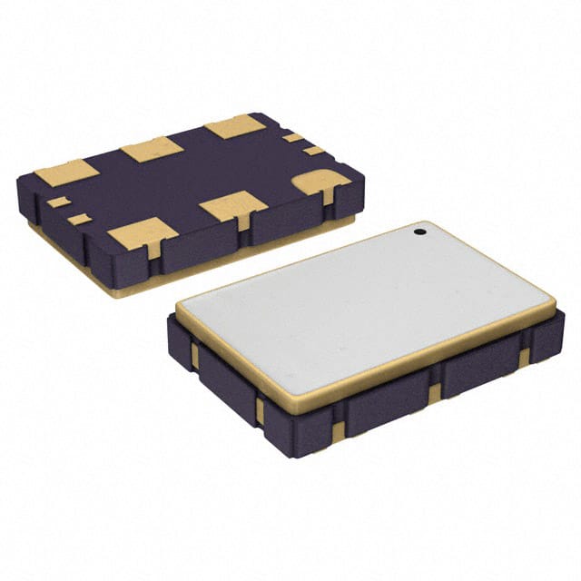
- Part No.:
- 8N3QV01AG-0081CDI
- Manufacturer:
- Renesas
- Category:
- Programmable Timers and Oscillators
- Package:
- 10-CLCC
- Datasheet:
-
 8N3QV01AG-0081CDI.pdf
- Description:
- IC OSC VCXO QD FREQ 10CLCC
- Quantity:
- Payment:

- Shipping:

Inventory:3,931
Please send an inquiry. Send us your inquiry, and we will respond immediately.
Product details
Overview
8N3QV01AG-0081CDI from Renesas Electronics is a quad-frequency programmable VCXO using fourth-generation FemtoClock® NG technology, delivering LVPECL differential output (15.476–866.67 MHz and 975–1300 MHz), ±4.5 to ±754.5 ppm absolute pull range, and 0.487 ps RMS phase jitter (12 kHz–20 MHz) at 156.25 MHz for wireless infrastructure timing applications.
For engineers reviewing the 8N3QV01AG-0081CDI datasheet, 8N3QV01AG-0081CDI pinout, 8N3QV01AG-0081CDI application, or 8N3QV01AG-0081CDI equivalent, this page provides verified package mapping (10-lead ceramic CD package), I²C-programmable PLL register architecture, FSEL0/FSEL1 default frequency selection logic, and validated LVPECL termination guidance per JEDEC standards.
Technical Context
The 8N3QV01AG-0081CDI integrates a 114.285 MHz 3rd-overtone crystal oscillator with a fractional-N PLL featuring 7-bit integer (MINT) and 18-bit fractional (MFRAC) feedback dividers, 2-bit pre-divider (P), and 7-bit post-divider (N), enabling precise frequency synthesis across two disjoint bands. Its VCO operates at 1950–2600 MHz.
Control is implemented via dual-path configuration: hardware-selectable default frequencies (FSEL0/FSEL1) map to four volatile I²C register sets (P₀–P₃, MINT₀–MINT₃, MFRAC₀–MFRAC₃, N₀–N₃), while runtime reprogramming via SDATA/SCLK supports custom APR and frequency tuning without power cycle - all under 2.5 V or 3.3 V supply.
Key Specifications
| Parameter | Value and Actual Design Meaning |
|---|---|
| Output Frequency Range | 15.476–866.67 MHz and 975–1300 MHz; supports telecom/datacom clocking with discrete band gaps optimized for SERDES and PHY layer timing. |
| RMS Phase Jitter (12 kHz–20 MHz) | 0.487 ps typical at 156.25 MHz; meets stringent OC-192/SONET and 10G Ethernet jitter budgets. |
| Absolute Pull Range (APR) | Programmable ±4.5 to ±754.5 ppm; enables fine-grained frequency lock in PLL-based synchronization systems. |
| Supply Voltage | 2.5 V ±5% or 3.3 V ±5%; dual-voltage compatibility simplifies integration into mixed-supply FPGA/ASIC platforms. |
| Operating Temperature | −40°C to +85°C industrial grade; qualified for base station RF units and carrier-grade networking equipment. |
| Output Interface | LVPECL differential (Q/nQ); requires 50 Ω termination to VCC − 2 V; supports >1 Gbps signaling integrity with <425 ps rise/fall time. |
| Frequency Resolution | 435.9 Hz ÷ N (N = post-divider); enables sub-Hz tuning granularity for precision frequency calibration loops. |
Pinout & Package
10-lead ceramic CLCC package (5 mm × 7 mm × 1.55 mm, RoHS 6-compliant, CD code), surface-mount, lead-free, with exposed metallized bottom pad per IPC-7351B NSMD land pattern.
| Pin/Terminal | Circuit Role | Design Meaning |
|---|---|---|
| 1 (VC) | VCXO control voltage input | Analog tuning port; gain programmable via ADC_GAIN[5:0] register; nominal range 0–VCC; linearity ±0.1% BSL. |
| 2 (OE) | Output enable (LVCMOS/LVTTL) | Asynchronous active-high control; drives Q/nQ into high-Z when low; internal pullup ensures default-enable behavior. |
| 3 (VEE) | Negative power supply | Ground reference for LVPECL outputs; must be connected directly to system ground plane with low-inductance path. |
| 4 (FSEL0), 5 (FSEL1) | Default frequency select inputs | LVCMOS/LVTTL inputs with internal pulldowns; select one of four factory-programmed PLL configurations at power-up. |
| 6 (Q), 7 (nQ) | Differential LVPECL clock outputs | Low-impedance emitter-follower outputs; require matched 50 Ω termination to VCC − 2 V for signal integrity and jitter performance. |
| 8 (VCC) | Positive power supply | 2.5 V or 3.3 V core supply; decoupling with 0.1 µF (device-side) + 10 µF recommended to suppress >10 kHz noise coupling into PLL. |
| 9 (SDATA) | I²C bidirectional data line | Open-drain output / LVCMOS input; requires external pullup; used to read/write P/M/N/ADC registers and APR settings. |
| 10 (SCLK) | I²C clock input | LVCMOS-compatible clock input; synchronizes register access; internal pullup ensures safe idle state. |
Key Features
| Feature | Design Value |
|---|---|
| Quad default frequency selection | FSEL0/FSEL1 pins directly map to four independent PLL register banks (P₀–P₃, MINT₀–MINT₃, etc.), enabling instant frequency switching without I²C transaction overhead. |
| Fractional-N PLL with delta-sigma modulation | Enables ultra-fine frequency resolution (sub-Hz) and robust noise shaping - critical for minimizing spurs in high-speed serial link clock recovery. |
| Volatile I²C register architecture | All configuration registers (frequency, APR, polarity) are RAM-based and reload factory defaults on power cycle - supports secure, non-persistent programming in field-upgradable systems. |
| LVPECL output with integrated biasing | Eliminates need for external current sources; designed for direct 50 Ω transmission-line drive with guaranteed VOH/VOL swing (0.55–1.0 Vpp) and <425 ps edge rates. |
| Wide APR programmability | ±4.5 to ±754.5 ppm range allows adaptation to diverse loop bandwidths and reference stability requirements - from telecom master clocks to packet network PTP grandmasters. |
Applications
| 5G Radio Unit Timing | Optical Transport Network (OTN) Line Cards |
|---|---|
Use Scenario: Synchronizing distributed massive MIMO antenna arrays requiring phase-coherent local oscillators referenced to a central PTP grandmaster. IC Role / Device Role / Timing Role: Programmable VCXO providing low-jitter, APR-tunable 156.25 MHz or 245.76 MHz clock to FPGA-based digital front-end processors. Use Value: 0.487 ps RMS phase jitter ensures EVM compliance; ±754.5 ppm APR accommodates temperature-induced drift in outdoor RU enclosures. | Use Scenario: Generating SONET/SDH and OTU4 line-rate clocks (e.g., 9.953 Gbps) in DWDM line cards where holdover stability and fast frequency agility are required. IC Role / Device Role / Timing Role: Quad-default VCXO supplying 155.52 MHz or 122.88 MHz to SerDes PHYs, with FSEL-driven switching during protection switchover events. Use Value: Sub-500 ps jitter preserves BER; I²C reprogrammability enables dynamic rate adaptation across OTU1/2/3/4 without hardware change. |
| Enterprise Switch Fabric Clocking | High-Frequency Trading (HFT) Network Appliances |
Use Scenario: Providing deterministic, low-latency clock distribution to multi-chip switch ASICs and packet buffer controllers in 10/25/100 GbE top-of-rack switches. IC Role / Device Role / Timing Role: LVPECL VCXO delivering 250 MHz or 312.5 MHz clock with tight duty cycle (45–55%) to minimize skew across parallel data paths. Use Value: 425 ps max rise/fall time and 55% max duty cycle deviation ensure setup/hold margin for DDR4/DDR5 interface timing. | Use Scenario: Enabling sub-microsecond timestamp alignment between FPGA-accelerated order matching engines and network interface cards in ultra-low-latency trading gateways. IC Role / Device Role / Timing Role: Precision VCXO generating 100 MHz or 125 MHz reference for TDCs and timestamp generators, with APR tuned to compensate for board-level thermal gradients. Use Value: ±20 ppm total stability (K-option compatible) and 0.614 ps RMS jitter (1 kHz–40 MHz) reduce timestamp uncertainty below 1 ns RMS. |
Equivalent & Alternatives
The following parts are listed as comparable options for similar VCXO applications.
| Alternative Part | Technical Difference | Application Difference | Selection Advice |
|---|---|---|---|
| 8N3QV01EG-0081CDI | Same package and pinout; differs only in option code: E = 3.3 V supply with ±50 ppm initial accuracy (vs. A = ±100 ppm). | Higher initial accuracy suits applications requiring tighter holdover stability without frequent I²C recalibration (e.g., mobile backhaul). | Select when ±50 ppm crystal tolerance is mandated by system-level timing budget, and 3.3 V supply is fixed. |
| 8N3QV01BG-0081CDI | Same package and pinout; differs only in option code: B = 2.5 V supply with ±100 ppm initial accuracy (vs. A = 3.3 V). | Lower supply voltage reduces power and EMI in dense, thermally constrained modules (e.g., compact optical modules). | Select when system uses 2.5 V rails exclusively and power efficiency is prioritized over voltage margin. |
Compared with 8N3QV01AG-0081CDI, the E- and B-variants retain identical programmability, jitter, and temperature range but trade initial accuracy or supply voltage - enabling optimization for holdover-critical or low-power deployments without redesigning layout or firmware.
Availability
8N3QV01AG-0081CDI is available at Aetrix Electronics and suitable for 5G radio unit timing, optical transport network line cards, enterprise switch fabric clocking, and high-frequency trading network appliances requiring stable component supply across extended industrial temperature ranges and long production lifecycles.
Supply support for 8N3QV01AG-0081CDI includes scheduled delivery planning, volume procurement assistance, BOM continuity management, traceable sourcing, and lifecycle availability coordination for OEM customers, industrial embedded developers, connected-device designers, and electronics production programs.
Manufacturer
Renesas Electronics Corporation is a global semiconductor leader specializing in microcontrollers, analog, power, and timing solutions, with deep expertise in high-performance clock generation and synchronization IP.
The 8N3QV01AG-0081CDI belongs to Renesas' FemtoClock® NG programmable VCXO family, engineered for wireless infrastructure, telecom, and networking equipment demanding ultra-low jitter, wide APR, and flexible frequency agility in compact ceramic packages.
FAQ
What is the default output frequency of the 8N3QV01AG-0081CDI at power-up?
The 8N3QV01AG-0081CDI has four factory-programmed default frequencies selected by FSEL0 and FSEL1 logic states; the specific values (e.g., 100/122.88/125/156.25 MHz) are encoded in the order code "0081" per Renesas' FemtoClock NG ordering guide. These are stored in volatile I²C registers and reload on power cycle unless overwritten.
Does the 8N3QV01AG-0081CDI support both 2.5 V and 3.3 V operation simultaneously?
No - the 8N3QV01AG-0081CDI operates exclusively at either 2.5 V ±5% or 3.3 V ±5%, as defined by its option code "A" (3.3 V). Supply voltage is fixed at manufacturing; mixing voltages risks damage. The device draws ~150 mA at 3.3 V and ~145 mA at 2.5 V, with separate VCC and VEE pins.
How is the absolute pull range (APR) programmed on the 8N3QV01AG-0081CDI?
The APR is programmed via the ADC_GAIN[5:0] register bits over I²C, setting oscillator gain from ±4.5 ppm to ±754.5 ppm in discrete steps. For example, ADC_GAIN = 000001 yields ±12.5 ppm at 3.3 V (7.57 ppm/V), while 111111 yields ±477.27 ppm. APR is independent of frequency selection and applies across the full output band.
Can the 8N3QV01AG-0081CDI generate frequencies outside the 15.476–866.67 MHz and 975–1300 MHz ranges?
No - the 8N3QV01AG-0081CDI's PLL architecture and VCO range (1950–2600 MHz) restrict valid output frequencies to those two disjoint bands. Frequencies between 866.67 MHz and 975 MHz are unsupported due to VCO and divider limitations; attempting them results in undefined or unstable output.
What termination is required for the LVPECL outputs of the 8N3QV01AG-0081CDI?
The 8N3QV01AG-0081CDI's Q/nQ LVPECL outputs require 50 Ω differential termination to VCC − 2 V. For 3.3 V operation, Figure 1A/B in the datasheet recommends 84 Ω pull-downs to 3.3 V and 125 Ω to ground; for 2.5 V, Figure 2C shows simplified 50 Ω terminations. Improper termination degrades jitter and causes signal integrity failures.
8N3QV01AG-0081CDI Specifications
- Product attributes
- Attribute value
- Manufacturer:
- Renesas
- Series:
- FemtoClock® NG
- Package/Case:
- 10-CLCC
- Packaging:
- Tray
- Product Status:
- Active
- Type:
- VCXO
- Count:
- -
- Frequency:
- 125MHz, 156.25MHz, 250MHz, 312.5MHz
- Voltage - Supply:
- 3.135V ~ 3.465V
- Current - Supply:
- 150 mA
- Operating Temperature:
- -40°C ~ 85°C
- Supplier Device Package:
- 10-CLCC (7x5)
- Mounting Type:
- Surface Mount
- Grade:
- -
- Qualification:
- -
8N3QV01AG-0081CDI FAQ
1.How can I place an order for 8N3QV01AG-0081CDI through Aetrix?
Please submit a Request for Quotation (RFQ) for 8N3QV01AG-0081CDI on Aetrix. Our sales agent will provide a competitive quotation and guide you through the order confirmation once you accept the terms.
2.Are the price and stock information for 8N3QV01AG-0081CDI reliable?
The price and inventory of 8N3QV01AG-0081CDI are updated periodically and may fluctuate due to market conditions. Stock and pricing data are typically refreshed every 24 hours. Quotation validity for 8N3QV01AG-0081CDI is usually 5 days.
3.What payment methods are accepted for 8N3QV01AG-0081CDI?
We accept Wire Transfer, PayPal, Credit Card, Western Union, MoneyGram, and Escrow for 8N3QV01AG-0081CDI transactions.
Note: Certain payment methods may incur a processing fee.
4.How is shipping managed for 8N3QV01AG-0081CDI?
8N3QV01AG-0081CDI orders can be shipped via leading logistics carriers, including DHL, UPS, FedEx, TNT, or Registered Mail.
Once your 8N3QV01AG-0081CDI order is processed, you will receive an email with the shipment details and tracking number.
Note: Tracking information may take up to 24 hours to appear. Express delivery typically takes 3–5 business days.
5.How can I obtain technical support or documentation for 8N3QV01AG-0081CDI?
For technical support, including 8N3QV01AG-0081CDI datasheets, pinout diagrams, or application guidance, please contact our engineering support team. They can provide detailed documentation and assistance for your 8N3QV01AG-0081CDI requirements.
6.How does Aetrix verify that 8N3QV01AG-0081CDI is sourced from the original manufacturer or authorized distributors?
All 8N3QV01AG-0081CDI products on Aetrix are procured from qualified distributors and authorized channels. Our dedicated quality assurance team conducts strict verification, including traceability checks and, if necessary, third-party testing. This ensures that 8N3QV01AG-0081CDI meets industry standards.
7.What is the process for return or replacement of 8N3QV01AG-0081CDI?
All 8N3QV01AG-0081CDI units undergo pre-shipment inspection (PSI). If there is an issue with 8N3QV01AG-0081CDI, returns or replacements are accepted under the following conditions:
1.Quantity discrepancies, incorrect items, or visible external defects (such as breakage or corrosion), acknowledged by Aetrix.
2.The issue is reported within 90 days of delivery.
3.The 8N3QV01AG-0081CDI part is unused and in its original packaging.
Return procedure for 8N3QV01AG-0081CDI:
1.Submit a request within 90 days.
2.Obtain a Return Material Authorization (RMA) from Aetrix.
8N3QV01AG-0081CDI Tags

-
NE555DR
Texas Instruments
-
SA555DR
Texas Instruments
-
NA555DR
Texas Instruments
-
SE555DR
Texas Instruments

-
NE555P
Texas Instruments

-
CD4541BM96
Texas Instruments

-
CD4541BE
Texas Instruments
-
TLC555QDR
Texas Instruments
-
TLC555IDR
Texas Instruments
-
TLC555QDRQ1
Texas Instruments

-
TPL5010DDCR
Texas Instruments
-
TLC555CP
Texas Instruments
Tech Hub

TTL and CMOS logic families differ in thresholds, loading, output drive, power and timing. This engineering guide compares 74HC and 74HCT, calculates noise margins and checks 3.3 V/5 V compatibility.

A practical engineering guide to 3.3V and 5V logic compatibility, input thresholds, resistor dividers, translator ICs, MOSFET level shifting, I2C pull-ups, timing limits and power-sequencing risks.

The 74HC595 uses push-pull logic outputs, while the TPIC6B595 uses 50 V open-drain DMOS sinks for higher-power loads. This guide compares timing, current limits, 3.3 V interfacing, load wiring, thermal…

The 74HC595 converts serial data into eight stable parallel outputs. This guide covers pin functions, shift and storage timing, OE and MR behavior, drive-current limits, cascading, voltage compatibilit…

A technical comparison of level-sensitive latches and edge-triggered flip-flops, covering timing windows, setup and hold limits, master–slave operation, time borrowing, race-through, HDL inference and…

A D latch stores one bit while Enable controls when data can pass. This reference covers gate-level operation, truth tables, transparency, setup and hold timing, LE versus OE, common ICs and practical …

An SR latch stores one bit through cross-coupled feedback. This engineering reference covers NOR and NAND implementations, truth tables, forbidden-state recovery, gated operation, switch debouncing, fa…

Latch circuits retain one bit through feedback. This technical reference covers SR and D latches, truth tables, transparency, timing limits, latch-versus-flip-flop behavior, applications and common log…

An engineering guide to LED driver operation, constant-current and constant-voltage outputs, linear and switching topologies, dimming, IC selection, calculations, replacement compatibility, and fault c…

Operational amplifier guide covering op amp basics, feedback, ideal vs real op amps, common configurations, buffer circuits, offset, bias current, gain-bandwidth, slew rate, rail-to-rail limits and sel…


