
 My Inquiry
 My Account


Renesas 8N3SV75EC-0026CDI8
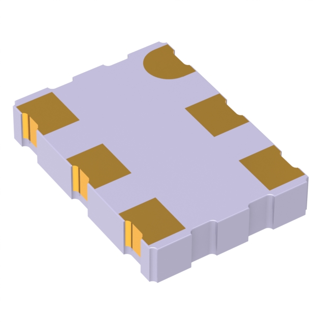
- Part No.:
- 8N3SV75EC-0026CDI8
- Manufacturer:
- Renesas
- Category:
- Programmable Timers and Oscillators
- Package:
- 6-CLCC
- Datasheet:
-
 8N3SV75EC-0026CDI8.pdf
- Description:
- IC OSC VCXO 311.04MHZ 6-CLCC
- Quantity:
- Payment:

- Shipping:

Inventory:1,860
Please send an inquiry. Send us your inquiry, and we will respond immediately.
Product details
Overview
8N3SV75EC-0026CDI8 from Renesas Electronics (formerly IDT) is a factory-programmed LVPECL voltage-controlled crystal oscillator (VCXO) with fourth-generation FemtoClock® NG PLL synthesis. It delivers 156.25 MHz output at 3.3 V supply, ±50 ppm total stability over –40°C to +85°C, 0.5 ps RMS phase jitter (12 kHz–20 MHz), and supports output enable control. Used in telecom line cards requiring precise, low-jitter clocking for SerDes and Ethernet PHYs.
For engineers reviewing the 8N3SV75EC-0026CDI8 datasheet, 8N3SV75EC-0026CDI8 pinout, 8N3SV75EC-0026CDI8 application, or 8N3SV75EC-0026CDI8 equivalent, key selection criteria include its programmable VCXO pull range (±50 ppm option), LVPECL differential output compliance, 6-pin ceramic 5 mm × 7 mm package, and guaranteed phase noise performance at 156.25 MHz.
Technical Context
The 8N3SV75EC-0026CDI8 integrates a 114.285 MHz fundamental-mode crystal with a fractional-N PLL featuring a 7-bit integer (MINT) and 18-bit fractional (MFRAC) feedback divider, enabling high-resolution frequency synthesis. Its VCO operates at 1950–2600 MHz before post-division.
It uses delta-sigma modulation for noise shaping and achieves low phase noise via high-reference-frequency multiplication. The device implements factory-configured VCXO control voltage polarity and absolute pull range (APR), with oscillator gain (KV) ranging from 7.57 to 477.27 ppm/V at 3.3 V.
Key Specifications
| Parameter | Value and Actual Design Meaning |
|---|---|
| Output Frequency | 156.25 MHz - precisely programmed default frequency for Ethernet 10GBase-R and OTU2 timing. |
| Output Interface | LVPECL differential - requires 50 Ω termination to VCC – 2 V; compatible with TI, Broadcom, and Marvell SerDes inputs. |
| RMS Phase Jitter | 0.5 ps (typical), 12 kHz–20 MHz integration - meets ITU-T G.823/G.825 and OIF CEI-6G jitter budgets. |
| Supply Voltage | 3.3 V ±5% - supports industrial-grade power rail with 130–160 mA current draw. |
| Operating Temp | –40°C to +85°C - qualified for base station and optical transport equipment ambient conditions. |
| Total Stability | ±63 ppm (10-year life) - combines ±50 ppm temp stability (Option E), ±10 ppm initial accuracy, and ±3 ppm aging. |
| Control Voltage Range | 0 to VCC - supports standard analog tuning with linear response (±0.1% BSL linearity). |
Pinout & Package
6-lead ceramic VFQFN package, 5 mm × 7 mm × 1.55 mm, RoHS-compliant (6/6), with exposed thermal pad (not electrically connected). Pin 1 index marked.
| Pin/Terminal | Circuit Role | Design Meaning |
|---|---|---|
| 1 (VC) | VCXO Control Voltage Input | Analog tuning input; 0–VCC range sets output frequency deviation within ±50 ppm APR. |
| 2 (OE) | Output Enable Input | LVCMOS/LVTTL-compatible active-high signal; drives Q/nQ into high-Z when low. |
| 3 (VEE) | Negative Power Supply | Ground reference for LVPECL outputs; must be connected to system ground plane. |
| 4 (Q), 5 (nQ) | Differential Clock Outputs | LVPECL-compliant complementary signals; require matched 50 Ω transmission lines and proper termination. |
| 6 (VCC) | Positive Power Supply | 3.3 V ±5% supply; decoupling with 0.1 µF capacitor required adjacent to pin. |
Key Features
| Feature | Design Value |
|---|---|
| FemtoClock® NG PLL Architecture | Enables 218 Hz frequency resolution and sub-0.6 ps phase jitter via fractional-N synthesis with delta-sigma noise shaping. |
| Factory-Programmed VCXO Pull Range | ±50 ppm APR (Option E) - eliminates field calibration and ensures consistent loop bandwidth in PLL-based clock recovery systems. |
| LVPECL Output Enable | Hardware-controlled OE pin allows dynamic clock gating without external logic, reducing system power during idle states. |
| High-Reference Crystal Oscillator | 114.285 MHz 3rd-overtone crystal minimizes multiplication-induced phase noise and improves jitter floor vs. fundamental-mode XO solutions. |
| Thermal Stability Optimization | Guaranteed ±50 ppm temperature stability (Option E) over –40°C to +85°C - suitable for uncooled wireless infrastructure deployments. |
Applications
| 10G/25G Ethernet Line Cards | OTN Transport Equipment |
|---|---|
Use Scenario: Providing reference clock to 10GBase-R or 25G Ethernet PHYs in carrier-grade aggregation switches. IC Role / Device Role / Timing Role: Primary low-jitter VCXO source for SerDes CDR circuits, synchronized to network timing via Synchronous Ethernet (SyncE). Use Value: 0.5 ps RMS phase jitter ensures bit error rate <1e–12 under worst-case channel loss and crosstalk conditions. | Use Scenario: Generating OTU2/OTU3 frame timing in DWDM line systems with hitless protection switching. IC Role / Device Role / Timing Role: Programmable VCXO referenced to BITS or PRC clocks, supporting holdover and fast reacquisition during network synchronization loss. Use Value: ±50 ppm APR enables tight loop bandwidth control in slave PLLs, minimizing wander accumulation per ITU-T G.813. |
| 5G Radio Unit (RU) Baseband | CPRI/eCPRI Fronthaul Timing |
Use Scenario: Delivering sample clock to wideband ADC/DAC in massive MIMO radio units operating in outdoor enclosures. IC Role / Device Role / Timing Role: Temperature-stable VCXO providing 156.25 MHz or harmonically related clocks for digital up/down conversion chains. Use Value: –40°C to +85°C operation and ±63 ppm 10-year stability ensure timing integrity across environmental extremes without recalibration. | Use Scenario: Synchronizing CPRI/eCPRI fronthaul links between BBU and remote radio heads in distributed antenna systems. IC Role / Device Role / Timing Role: Low-phase-noise VCXO used as local oscillator in fronthaul transceivers, locked to master clock via IEEE 1588 or SyncE. Use Value: Sub-1 ps cycle-to-cycle jitter prevents timing misalignment that would degrade IQ constellation fidelity in 256-QAM transmissions. |
Equivalent & Alternatives
The following parts are listed as comparable options for similar VCXO applications.
| Alternative Part | Technical Difference | Application Difference | Selection Advice |
|---|---|---|---|
| 8N3SV75EC-0027CDI8 | Same package, same electrical specs, but factory-programmed to 125 MHz output frequency. | Used where 125 MHz is required for PCIe Gen3 or SATA Gen3 reference clocks instead of 156.25 MHz. | Select only if target system requires 125 MHz; no PCB or firmware changes needed beyond frequency configuration. |
| Si510-PROG | Programmable I2C-configurable XO (not VCXO); 0.8 ps phase jitter at 156.25 MHz; 3.3 V only; 5 mm × 7 mm QFN. | Lacks analog VCXO tuning capability; suited for fixed-frequency applications with digital reconfiguration needs. | Choose when design requires field-programmability or I2C-based frequency agility, not analog voltage tuning. |
Compared with 8N3SV75EC-0026CDI8, the 0027 variant offers identical form-factor and stability but targets different data rates, while Si510-PROG trades VCXO functionality for digital configurability-making it unsuitable for analog PLL lock loops but advantageous for multi-protocol systems needing runtime frequency updates.
Availability
8N3SV75EC-0026CDI8 is available at Aetrix Electronics and suitable for telecom infrastructure, optical transport, and 5G wireless baseband applications requiring stable component supply, long-lifecycle support, and guaranteed phase noise performance.
Supply support for 8N3SV75EC-0026CDI8 includes scheduled delivery planning, volume procurement assistance, BOM continuity management, traceable sourcing, and lifecycle availability coordination for OEM customers, industrial embedded developers, connected-device designers, and electronics production programs.
Manufacturer
Renesas Electronics Corporation is a global semiconductor leader delivering microcontrollers, analog power, and timing solutions for automotive, industrial, and communications markets.
The IDT8N3SV75 product line was developed by Integrated Device Technology (acquired by Renesas in 2019) to address high-performance timing needs in next-generation wired and wireless infrastructure, emphasizing ultra-low jitter, programmable VCXO flexibility, and extended temperature reliability.
FAQ
What is the factory-programmed output frequency of the 8N3SV75EC-0026CDI8?
The 8N3SV75EC-0026CDI8 is factory-programmed to deliver a precise 156.25 MHz LVPECL differential output. This frequency aligns with industry standards for 10G Ethernet (10GBase-R), OTU2 framing, and CPRI/eCPRI fronthaul timing. The device does not support field reprogramming - its frequency and VCXO pull range are permanently set during manufacturing per order code 0026.
Does the 8N3SV75EC-0026CDI8 support both 2.5 V and 3.3 V supply voltages?
No, the 8N3SV75EC-0026CDI8 is specifically configured for 3.3 V ±5% operation (Option Code E). Its internal regulators and LVPECL driver stages are optimized for this supply; applying 2.5 V will result in noncompliant output voltage swing and degraded jitter performance. For 2.5 V operation, select part numbers with Option Codes B, F, or L (e.g., 8N3SV75FC-xxxx).
How is the VCXO pull range implemented in the 8N3SV75EC-0026CDI8?
The 8N3SV75EC-0026CDI8 implements a factory-programmed absolute pull range (APR) of ±50 ppm via internal register settings controlling the PLL's oscillator gain (KV) and control voltage scaling. With VC applied from 0 to VCC, the output frequency deviates linearly within ±50 ppm of 156.25 MHz. This APR is fixed and cannot be altered post-manufacture - it is defined by the "E" option code and order-specific programming.
What termination scheme is required for the LVPECL outputs of the 8N3SV75EC-0026CDI8?
The 8N3SV75EC-0026CDI8 LVPECL outputs (Q and nQ) require DC-coupled 50 Ω termination to VCC – 2 V. For 3.3 V operation, this equals 1.3 V. Recommended layouts use dual 84 Ω resistors (Figure 1A) or 125 Ω resistors (Figure 1B) per output leg. AC coupling is not supported. Improper termination causes signal integrity degradation, increased jitter, and duty cycle distortion beyond the specified 45–55% range.
Can the 8N3SV75EC-0026CDI8 be used in place of a fixed-frequency XO?
Yes, the 8N3SV75EC-0026CDI8 can function as a high-stability XO by holding the VC pin at VCC/2 (1.65 V), which centers the output at the nominal 156.25 MHz frequency with minimal drift. Its ±50 ppm total stability over 10 years matches or exceeds many standalone XOs. However, unlike a pure XO, it retains full VCXO capability - enabling fine-tuning, holdover compensation, or synchronization to external references when needed.
8N3SV75EC-0026CDI8 Specifications
- Product attributes
- Attribute value
- Manufacturer:
- Renesas
- Series:
- FemtoClock® NG
- Package/Case:
- 6-CLCC
- Packaging:
- Tape & Reel (TR)
- Product Status:
- Active
- Type:
- VCXO
- Count:
- -
- Frequency:
- 311.04MHz
- Voltage - Supply:
- 3.135V ~ 3.465V
- Current - Supply:
- 130 mA
- Operating Temperature:
- -40°C ~ 85°C
- Supplier Device Package:
- 6-CLCC (7x5)
- Mounting Type:
- Surface Mount
- Grade:
- -
- Qualification:
- -
8N3SV75EC-0026CDI8 FAQ
1.How can I place an order for 8N3SV75EC-0026CDI8 through Aetrix?
Please submit a Request for Quotation (RFQ) for 8N3SV75EC-0026CDI8 on Aetrix. Our sales agent will provide a competitive quotation and guide you through the order confirmation once you accept the terms.
2.Are the price and stock information for 8N3SV75EC-0026CDI8 reliable?
The price and inventory of 8N3SV75EC-0026CDI8 are updated periodically and may fluctuate due to market conditions. Stock and pricing data are typically refreshed every 24 hours. Quotation validity for 8N3SV75EC-0026CDI8 is usually 5 days.
3.What payment methods are accepted for 8N3SV75EC-0026CDI8?
We accept Wire Transfer, PayPal, Credit Card, Western Union, MoneyGram, and Escrow for 8N3SV75EC-0026CDI8 transactions.
Note: Certain payment methods may incur a processing fee.
4.How is shipping managed for 8N3SV75EC-0026CDI8?
8N3SV75EC-0026CDI8 orders can be shipped via leading logistics carriers, including DHL, UPS, FedEx, TNT, or Registered Mail.
Once your 8N3SV75EC-0026CDI8 order is processed, you will receive an email with the shipment details and tracking number.
Note: Tracking information may take up to 24 hours to appear. Express delivery typically takes 3–5 business days.
5.How can I obtain technical support or documentation for 8N3SV75EC-0026CDI8?
For technical support, including 8N3SV75EC-0026CDI8 datasheets, pinout diagrams, or application guidance, please contact our engineering support team. They can provide detailed documentation and assistance for your 8N3SV75EC-0026CDI8 requirements.
6.How does Aetrix verify that 8N3SV75EC-0026CDI8 is sourced from the original manufacturer or authorized distributors?
All 8N3SV75EC-0026CDI8 products on Aetrix are procured from qualified distributors and authorized channels. Our dedicated quality assurance team conducts strict verification, including traceability checks and, if necessary, third-party testing. This ensures that 8N3SV75EC-0026CDI8 meets industry standards.
7.What is the process for return or replacement of 8N3SV75EC-0026CDI8?
All 8N3SV75EC-0026CDI8 units undergo pre-shipment inspection (PSI). If there is an issue with 8N3SV75EC-0026CDI8, returns or replacements are accepted under the following conditions:
1.Quantity discrepancies, incorrect items, or visible external defects (such as breakage or corrosion), acknowledged by Aetrix.
2.The issue is reported within 90 days of delivery.
3.The 8N3SV75EC-0026CDI8 part is unused and in its original packaging.
Return procedure for 8N3SV75EC-0026CDI8:
1.Submit a request within 90 days.
2.Obtain a Return Material Authorization (RMA) from Aetrix.
8N3SV75EC-0026CDI8 Tags

-
NE555DR
Texas Instruments
-
SA555DR
Texas Instruments
-
NA555DR
Texas Instruments
-
SE555DR
Texas Instruments

-
NE555P
Texas Instruments

-
CD4541BM96
Texas Instruments

-
CD4541BE
Texas Instruments
-
TLC555QDR
Texas Instruments
-
TLC555IDR
Texas Instruments
-
TLC555QDRQ1
Texas Instruments

-
TPL5010DDCR
Texas Instruments
-
TLC555CP
Texas Instruments
Tech Hub

TTL and CMOS logic families differ in thresholds, loading, output drive, power and timing. This engineering guide compares 74HC and 74HCT, calculates noise margins and checks 3.3 V/5 V compatibility.

A practical engineering guide to 3.3V and 5V logic compatibility, input thresholds, resistor dividers, translator ICs, MOSFET level shifting, I2C pull-ups, timing limits and power-sequencing risks.

The 74HC595 uses push-pull logic outputs, while the TPIC6B595 uses 50 V open-drain DMOS sinks for higher-power loads. This guide compares timing, current limits, 3.3 V interfacing, load wiring, thermal…

The 74HC595 converts serial data into eight stable parallel outputs. This guide covers pin functions, shift and storage timing, OE and MR behavior, drive-current limits, cascading, voltage compatibilit…

A technical comparison of level-sensitive latches and edge-triggered flip-flops, covering timing windows, setup and hold limits, master–slave operation, time borrowing, race-through, HDL inference and…

A D latch stores one bit while Enable controls when data can pass. This reference covers gate-level operation, truth tables, transparency, setup and hold timing, LE versus OE, common ICs and practical …

An SR latch stores one bit through cross-coupled feedback. This engineering reference covers NOR and NAND implementations, truth tables, forbidden-state recovery, gated operation, switch debouncing, fa…

Latch circuits retain one bit through feedback. This technical reference covers SR and D latches, truth tables, transparency, timing limits, latch-versus-flip-flop behavior, applications and common log…

An engineering guide to LED driver operation, constant-current and constant-voltage outputs, linear and switching topologies, dimming, IC selection, calculations, replacement compatibility, and fault c…

Operational amplifier guide covering op amp basics, feedback, ideal vs real op amps, common configurations, buffer circuits, offset, bias current, gain-bandwidth, slew rate, rail-to-rail limits and sel…


