
 My Inquiry
 My Account


Renesas 8N4SV75KC-0076CDI8
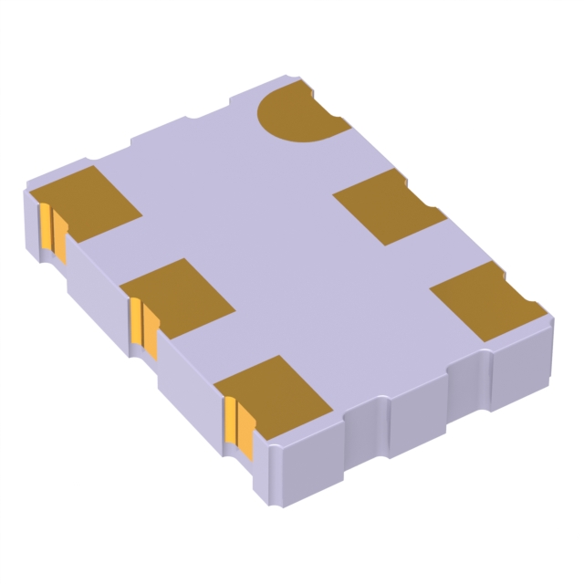
- Part No.:
- 8N4SV75KC-0076CDI8
- Manufacturer:
- Renesas
- Category:
- Programmable Timers and Oscillators
- Package:
- 6-CLCC
- Datasheet:
-
 8N4SV75KC-0076CDI8.pdf
- Description:
- IC OSC VCXO 200MHZ 6-CLCC
- Quantity:
- Payment:

- Shipping:

Inventory:2,609
Please send an inquiry. Send us your inquiry, and we will respond immediately.
Product details
Overview
8N4SV75KC-0076CDI8 from Renesas Electronics (formerly IDT) is a factory-programmed LVDS voltage-controlled crystal oscillator (VCXO) with fourth-generation FemtoClock® NG PLL synthesis. It delivers programmable output frequencies from 15.476 MHz to 866.67 MHz and 975 MHz to 1,300 MHz, ±20 ppm total stability over –40°C to +85°C, 0.53 ps RMS phase jitter at 156.25 MHz (12 kHz–20 MHz), and operates from 2.5 V or 3.3 V supply. It serves as a low-jitter timing source in wireless baseband units and high-speed SerDes clocking.
For engineers reviewing the 8N4SV75KC-0076CDI8 datasheet, 8N4SV75KC-0076CDI8 pinout, 8N4SV75KC-0076CDI8 application, or 8N4SV75KC-0076CDI8 equivalent, key selection criteria include its dual-band frequency coverage, factory-set ±20 ppm stability (Option K), LVDS differential output compliance, OE-enabled output control, and ceramic 5 mm × 7 mm × 1.55 mm CD package suitability for space-constrained telecom modules.
Technical Context
The 8N4SV75KC-0076CDI8 integrates a 114.285 MHz 3rd-overtone crystal oscillator with a fractional-N PLL featuring a 7-bit integer plus 18-bit fractional feedback divider (MINT/MFRAC), 2-bit pre-divider (P), and 7-bit post-divider (N). Its FemtoClock® NG VCO operates at 1950–2600 MHz, enabling high-resolution synthesis with ≤218 Hz frequency step size.
It supports factory-configured VCXO pull range (±4.5 to ±754.5 ppm) and control voltage polarity, with oscillator gain tunable from 7.57 to 477.27 ppm/V (at 3.3 V) and modulation bandwidth of 100 kHz. The device uses delta-sigma noise shaping to minimize phase noise, achieving –113 dBc/Hz at 10 kHz offset from 156.25 MHz carrier.
Key Specifications
| Parameter | Value and Actual Design Meaning |
|---|---|
| Output Type | LVDS differential pair (Q/nQ), compliant with ANSI TIA/EIA-644-A |
| Frequency Range | 15.476–866.67 MHz and 975–1300 MHz; supports precise channel spacing in 5G NR and CPRI systems |
| RMS Phase Jitter | 0.53 ps typical at 156.25 MHz (12 kHz–20 MHz); meets SONET OC-192 and 10G Ethernet jitter budgets |
| Total Frequency Stability | ±20 ppm over –40°C to +85°C (Option K); ensures timing margin in outdoor wireless infrastructure |
| Supply Voltage | 2.5 V ±5% or 3.3 V ±5%; compatible with mixed-voltage FPGA/ASIC power domains |
| Startup Time | 15 ms maximum; enables fast system boot and dynamic clock switching |
| Control Interface | LVCMOS/LVTTL-compatible OE input (pin 2); allows synchronous enable/disable of LVDS outputs |
Pinout & Package
Package: RoHS-compliant 6-lead ceramic CD package (5 mm × 7 mm × 1.55 mm), industrial temperature grade (–40°C to +85°C).
| Pin/Terminal | Circuit Role | Design Meaning |
|---|---|---|
| 1 - VC | VCXO control voltage input | Accepts 0–VDD tuning voltage; sets output frequency within factory-programmed APR (±20 ppm) |
| 2 - OE | Output enable input | LVCMOS/LVTTL logic level; drives Q/nQ into high-Z when low; default-active-high |
| 3 - GND | Power ground | Reference for all analog and digital circuitry; requires low-inductance connection to PCB ground plane |
| 4 - Q | Differential LVDS output (+) | 247–454 mV differential swing; requires 100 Ω termination at receiver for impedance matching |
| 5 - nQ | Differential LVDS output (–) | Complementary to Q; defines LVDS common-mode voltage (1.13–1.31 V) and duty cycle (45–55%) |
| 6 - VDD | Power supply input | Accepts 2.5 V or 3.3 V; requires local 0.1 µF + 10 µF decoupling per datasheet layout guidelines |
Key Features
| Feature | Design Value |
|---|---|
| Fractional-N PLL with delta-sigma modulator | Enables <218 Hz frequency resolution and low close-in phase noise without external loop filter components |
| Factory-programmed ±20 ppm stability (Option K) | Guarantees tight timing margin for IEEE 1588 PTP grandmaster clocks and OTN framers |
| LVDS output with 0.53 ps RMS jitter @ 156.25 MHz | Meets ITU-T G.823/G.824 wander and jitter masks for SDH/SONET line cards |
| OE-controlled high-impedance output state | Allows hot-swap clock source switching and power-aware clock gating in multi-processor SoCs |
| 5 mm × 7 mm ceramic hermetic package | Provides superior thermal stability and long-term aging performance vs. plastic packages in base station environments |
Applications
| Wireless Baseband Unit | Optical Transport Network (OTN) |
|---|---|
Use Scenario: Synchronizing ADC/DAC sampling clocks and FPGA fabric in massive MIMO radio units operating at -40°C to +85°C ambient. IC Role / Device Role / Timing Role: Primary VCXO providing low-jitter reference for JESD204B serializer/deserializer links and numerically controlled oscillators (NCOs). Use Value: 0.53 ps RMS jitter ensures <10–12 BER in 28 Gbps PAM4 interfaces; ±20 ppm stability maintains frame alignment across temperature cycling. | Use Scenario: Clocking OTU-2/OTU-3 framer ASICs in metro DWDM line cards requiring strict G.823/G.824 compliance. IC Role / Device Role / Timing Role: Stratum-3E-compliant timing source feeding clock data recovery (CDR) circuits and forward error correction (FEC) engines. Use Value: Dual-band support enables single part number for both 10.709 GHz and 43.018 GHz OTN line rates; LVDS drive strength matches TI/ADI CDR input sensitivity. |
| High-Speed Test Equipment | 5G Small Cell Backhaul |
Use Scenario: Generating precise stimulus clocks for bit-error-rate testers (BERTs) and arbitrary waveform generators (AWGs) used in 5G NR physical layer validation. IC Role / Device Role / Timing Role: Programmable reference oscillator enabling sweep-mode frequency agility across FR1 and FR2 bands. Use Value: 218 Hz resolution allows exact replication of channel raster frequencies (e.g., 30 kHz, 60 kHz); 15 ms startup supports automated test sequencing. | Use Scenario: Providing synchronization for eCPRI interface between distributed unit (DU) and active antenna unit (AAU) in virtualized RAN deployments. IC Role / Device Role / Timing Role: Boundary clock source meeting IEEE 1588v2 Class C requirements for sub-100 ns time error in fronthaul networks. Use Value: Ceramic package and ±20 ppm stability ensure holdover accuracy during GNSS signal loss; LVDS output drives long traces to remote PHYs. |
Equivalent & Alternatives
The following parts are listed as comparable options for similar VCXO applications.
| Alternative Part | Technical Difference | Application Difference | Selection Advice |
|---|---|---|---|
| Si510-PROG | CMOS output only; no LVDS; 10–210 MHz range; ±50 ppm stability (industrial) | Limited to lower-frequency control-plane clocks; unsuitable for high-speed SerDes | Select only if LVDS is not required and frequency stays below 210 MHz |
| AK2-156.250MHZ-E | Fixed-frequency LVDS XO (no VCXO function); ±25 ppm stability; same CD package | No voltage tuning capability; cannot compensate for system-level drift or PTP servo adjustments | Choose when absolute frequency stability suffices and no dynamic pull-range is needed |
Compared with 8N4SV75KC-0076CDI8, Si510-PROG lacks LVDS drive and high-frequency coverage, while AK2-156.250MHZ-E omits VCXO functionality entirely-making 8N4SV75KC-0076CDI8 the sole option for programmable, LVDS-based, ±20 ppm-stable VCXO operation above 150 MHz in telecom infrastructure.
Availability
8N4SV75KC-0076CDI8 is available at Aetrix Electronics and suitable for wireless infrastructure, optical transport network equipment, and high-speed test instrumentation requiring stable component supply, guaranteed long-term availability, and traceable RoHS-compliant sourcing.
Supply support for 8N4SV75KC-0076CDI8 includes scheduled delivery planning, volume procurement assistance, BOM continuity management, traceable sourcing, and lifecycle availability coordination for OEM customers, industrial embedded developers, connected-device designers, and electronics production programs.
Manufacturer
Renesas Electronics Corporation is a global semiconductor leader delivering trusted embedded solutions for automotive, industrial, infrastructure, and IoT markets, formed through the acquisition of IDT in 2019.
The 8N4SV75 series belongs to Renesas' FemtoClock® NG programmable timing portfolio, engineered specifically for high-frequency, low-jitter clock generation in next-generation wireless, networking, and test equipment where phase noise and stability are critical.
FAQ
What is the factory-programmed frequency and pull range for 8N4SV75KC-0076CDI8?
The 8N4SV75KC-0076CDI8 is programmed with Option K (±20 ppm total stability) and default configuration code "0076", indicating a specific factory-set frequency and absolute pull range (APR) within the supported bands (15.476–866.67 MHz or 975–1300 MHz). Exact values are defined in the ordering documentation and must be confirmed via Renesas' FemtoClock NG Programming Guide or order-specific configuration report. The 8N4SV75KC-0076CDI8 does not support field reprogramming.
Does 8N4SV75KC-0076CDI8 support both 2.5 V and 3.3 V supply voltages simultaneously?
No. The 8N4SV75KC-0076CDI8 operates from either 2.5 V ±5% or 3.3 V ±5%, but not both concurrently. The supply voltage is selected at factory programming and fixed for the life of the device. The 8N4SV75KC-0076CDI8 datasheet specifies separate DC characteristics tables for each voltage; users must verify VDD rating on the device marking and match it to their board's power rail. Incorrect voltage may cause functional failure or accelerated aging.
How is the output enable (OE) pin configured on 8N4SV75KC-0076CDI8?
On the 8N4SV75KC-0076CDI8, OE is an LVCMOS/LVTTL-compatible input on pin 2 with internal pull-up resistor (~50 kΩ). When OE = high (≥2.0 V at 3.3 V supply), Q/nQ outputs are active; when OE = low (≤0.8 V), outputs enter high-impedance state. The 8N4SV75KC-0076CDI8 does not support inverted OE logic-the "V76" suffix denotes standard active-high OE, unlike "V75" which uses active-low OE.
Can 8N4SV75KC-0076CDI8 be used as a drop-in replacement for 8N4SV75EC-0076CDI8?
No. While both share the same package and pinout, 8N4SV75KC-0076CDI8 (Option K, ±20 ppm) and 8N4SV75EC-0076CDI8 (Option E, ±50 ppm) differ in factory-programmed frequency stability, oscillator gain, and thermal drift behavior. Substituting them without redesign risks violating system-level jitter or wander specifications. The 8N4SV75KC-0076CDI8 must be validated independently in the target application, especially for Stratum-3E or IEEE 1588 use cases.
What is the recommended termination for the LVDS outputs of 8N4SV75KC-0076CDI8?
The 8N4SV75KC-0076CDI8 LVDS outputs (Q/nQ) require a 100 Ω differential termination resistor placed as close as possible to the receiver input. This matches the typical PCB differential impedance and minimizes reflections. Per Renesas' Application Information, a point-to-point topology with 100 Ω parallel termination is standard; optional center-tap capacitance (≈50 pF) may be added to suppress common-mode noise. The 8N4SV75KC-0076CDI8 output driver is designed for this load and will not meet jitter specs with unterminated or mismatched traces.
8N4SV75KC-0076CDI8 Specifications
- Product attributes
- Attribute value
- Manufacturer:
- Renesas
- Series:
- FemtoClock® NG
- Package/Case:
- 6-CLCC
- Packaging:
- Tape & Reel (TR)
- Product Status:
- Active
- Type:
- VCXO
- Count:
- -
- Frequency:
- 200MHz
- Voltage - Supply:
- 3.135V ~ 3.465V
- Current - Supply:
- 140 mA
- Operating Temperature:
- -40°C ~ 85°C
- Supplier Device Package:
- 6-CLCC (7x5)
- Mounting Type:
- Surface Mount
- Grade:
- -
- Qualification:
- -
8N4SV75KC-0076CDI8 FAQ
1.How can I place an order for 8N4SV75KC-0076CDI8 through Aetrix?
Please submit a Request for Quotation (RFQ) for 8N4SV75KC-0076CDI8 on Aetrix. Our sales agent will provide a competitive quotation and guide you through the order confirmation once you accept the terms.
2.Are the price and stock information for 8N4SV75KC-0076CDI8 reliable?
The price and inventory of 8N4SV75KC-0076CDI8 are updated periodically and may fluctuate due to market conditions. Stock and pricing data are typically refreshed every 24 hours. Quotation validity for 8N4SV75KC-0076CDI8 is usually 5 days.
3.What payment methods are accepted for 8N4SV75KC-0076CDI8?
We accept Wire Transfer, PayPal, Credit Card, Western Union, MoneyGram, and Escrow for 8N4SV75KC-0076CDI8 transactions.
Note: Certain payment methods may incur a processing fee.
4.How is shipping managed for 8N4SV75KC-0076CDI8?
8N4SV75KC-0076CDI8 orders can be shipped via leading logistics carriers, including DHL, UPS, FedEx, TNT, or Registered Mail.
Once your 8N4SV75KC-0076CDI8 order is processed, you will receive an email with the shipment details and tracking number.
Note: Tracking information may take up to 24 hours to appear. Express delivery typically takes 3–5 business days.
5.How can I obtain technical support or documentation for 8N4SV75KC-0076CDI8?
For technical support, including 8N4SV75KC-0076CDI8 datasheets, pinout diagrams, or application guidance, please contact our engineering support team. They can provide detailed documentation and assistance for your 8N4SV75KC-0076CDI8 requirements.
6.How does Aetrix verify that 8N4SV75KC-0076CDI8 is sourced from the original manufacturer or authorized distributors?
All 8N4SV75KC-0076CDI8 products on Aetrix are procured from qualified distributors and authorized channels. Our dedicated quality assurance team conducts strict verification, including traceability checks and, if necessary, third-party testing. This ensures that 8N4SV75KC-0076CDI8 meets industry standards.
7.What is the process for return or replacement of 8N4SV75KC-0076CDI8?
All 8N4SV75KC-0076CDI8 units undergo pre-shipment inspection (PSI). If there is an issue with 8N4SV75KC-0076CDI8, returns or replacements are accepted under the following conditions:
1.Quantity discrepancies, incorrect items, or visible external defects (such as breakage or corrosion), acknowledged by Aetrix.
2.The issue is reported within 90 days of delivery.
3.The 8N4SV75KC-0076CDI8 part is unused and in its original packaging.
Return procedure for 8N4SV75KC-0076CDI8:
1.Submit a request within 90 days.
2.Obtain a Return Material Authorization (RMA) from Aetrix.
8N4SV75KC-0076CDI8 Tags

-
NE555DR
Texas Instruments
-
SA555DR
Texas Instruments
-
NA555DR
Texas Instruments
-
SE555DR
Texas Instruments

-
NE555P
Texas Instruments

-
CD4541BM96
Texas Instruments

-
CD4541BE
Texas Instruments
-
TLC555QDR
Texas Instruments
-
TLC555IDR
Texas Instruments
-
TLC555QDRQ1
Texas Instruments

-
TPL5010DDCR
Texas Instruments
-
TLC555CP
Texas Instruments
Tech Hub

TTL and CMOS logic families differ in thresholds, loading, output drive, power and timing. This engineering guide compares 74HC and 74HCT, calculates noise margins and checks 3.3 V/5 V compatibility.

A practical engineering guide to 3.3V and 5V logic compatibility, input thresholds, resistor dividers, translator ICs, MOSFET level shifting, I2C pull-ups, timing limits and power-sequencing risks.

The 74HC595 uses push-pull logic outputs, while the TPIC6B595 uses 50 V open-drain DMOS sinks for higher-power loads. This guide compares timing, current limits, 3.3 V interfacing, load wiring, thermal…

The 74HC595 converts serial data into eight stable parallel outputs. This guide covers pin functions, shift and storage timing, OE and MR behavior, drive-current limits, cascading, voltage compatibilit…

A technical comparison of level-sensitive latches and edge-triggered flip-flops, covering timing windows, setup and hold limits, master–slave operation, time borrowing, race-through, HDL inference and…

A D latch stores one bit while Enable controls when data can pass. This reference covers gate-level operation, truth tables, transparency, setup and hold timing, LE versus OE, common ICs and practical …

An SR latch stores one bit through cross-coupled feedback. This engineering reference covers NOR and NAND implementations, truth tables, forbidden-state recovery, gated operation, switch debouncing, fa…

Latch circuits retain one bit through feedback. This technical reference covers SR and D latches, truth tables, transparency, timing limits, latch-versus-flip-flop behavior, applications and common log…

An engineering guide to LED driver operation, constant-current and constant-voltage outputs, linear and switching topologies, dimming, IC selection, calculations, replacement compatibility, and fault c…

Operational amplifier guide covering op amp basics, feedback, ideal vs real op amps, common configurations, buffer circuits, offset, bias current, gain-bandwidth, slew rate, rail-to-rail limits and sel…


