
 My Inquiry
 My Account


Renesas 8N4SV76EC-0065CDI
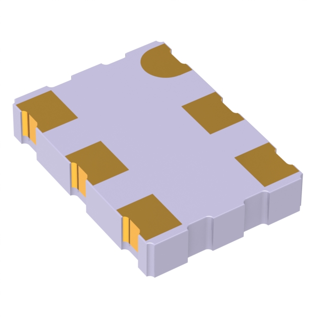
- Part No.:
- 8N4SV76EC-0065CDI
- Manufacturer:
- Renesas
- Category:
- Programmable Timers and Oscillators
- Package:
- 6-CLCC
- Datasheet:
-
 8N4SV76EC-0065CDI.pdf
- Description:
- IC OSC VCXO 212.5MHZ 6-CLCC
- Quantity:
- Payment:

- Shipping:

Inventory:3,260
Please send an inquiry. Send us your inquiry, and we will respond immediately.
Product details
Overview
8N4SV76EC-0065CDI from Integrated Device Technology is a factory-programmed LVDS voltage-controlled crystal oscillator (VCXO) with fourth-generation FemtoClock® NG PLL architecture, supporting output frequencies from 15.476 MHz to 866.67 MHz and 975 MHz to 1,300 MHz, ±20 ppm total stability over –40°C to +85°C, RMS phase jitter of 0.53 ps (156.25 MHz, 12 kHz–20 MHz), and 2.5 V/3.3 V dual-supply compatibility - deployed in wireless infrastructure baseband timing and high-speed SerDes clocking.
For engineers reviewing the 8N4SV76EC-0065CDI datasheet, 8N4SV76EC-0065CDI pinout, 8N4SV76EC-0065CDI application, or 8N4SV76EC-0065CDI equivalent, key selection criteria include its programmable APR (±4.5 to ±754.5 ppm), LVDS differential output compliance, nOE-controlled tri-state capability, and ceramic 5 mm × 7 mm × 1.55 mm CD package with industrial temperature rating.
Technical Context
The 8N4SV76EC-0065CDI integrates a 114.285 MHz third-overtone crystal oscillator driving a fractional-N PLL with 7-bit integer (MINT) and 18-bit fractional (MFRAC) feedback dividers, enabling frequency resolution ≤218 Hz. Its VCO operates at 1950–2600 MHz, followed by post-divider N and pre-divider P for precise output synthesis.
It implements factory-configured VCXO control voltage polarity and absolute pull-range (APR), with oscillator gain (KV) ranging 7.57–477.27 ppm/V (3.3 V) or 10–630 ppm/V (2.5 V), and supports LVCMOS/LVTTL-compatible nOE input for output enable/disable control with internal pulldown resistors.
Key Specifications
| Parameter | Value and Actual Design Meaning |
|---|---|
| Output Frequency Range | 15.476–866.67 MHz and 975–1300 MHz - covers Ethernet, CPRI, OTU4, and high-speed ADC/DAC sampling clocks. |
| RMS Phase Jitter | 0.53 ps typical @ 156.25 MHz (12 kHz–20 MHz) - meets stringent OC-192 and 10G/25G Ethernet jitter budgets. |
| Frequency Resolution | ≤218 Hz - enables exact alignment with system reference frequencies without external divider chains. |
| Absolute Pull Range (APR) | Programmable ±4.5 to ±754.5 ppm - supports wide-loop PLLs and dynamic frequency adjustment in sync-over-packet systems. |
| Supply Voltage | 2.5 V or 3.3 V ±5% - allows direct integration into mixed-voltage FPGA/ASIC power domains without level-shifting. |
| Operating Temperature | –40°C to +85°C - qualified for outdoor wireless radio units and telecom line cards. |
| Package | RoHS-compliant 6-lead ceramic VFQFN, 5 mm × 7 mm × 1.55 mm (CD) - surface-mount compatible with automated assembly and thermal cycling reliability. |
Pinout & Package
6-lead ceramic VFQFN package (IDT CD package), 5 mm × 7 mm × 1.55 mm, lead-free (RoHS 6), exposed pad not electrically connected.
| Pin/Terminal | Circuit Role | Design Meaning |
|---|---|---|
| VC | VCXO Control Voltage Input | Analog tuning input (0–VDD); sets output frequency within APR; impedance 500 kΩ; linearity ±0.1% BSL. |
| nOE | LVCMOS/LVTTL Output Enable (active-low) | Pulldown-enabled input; drives Q/nQ outputs to high-impedance when asserted; VIH ≥1.7 V (2.5 V supply). |
| GND | Power Supply Ground | Dedicated ground return for core and output circuitry; must be low-inductance connection to minimize jitter coupling. |
| Q, nQ | Differential LVDS Clock Outputs | True/complement LVDS pair (247–454 mV diff swing, 1.13–1.31 V common-mode); requires 100 Ω differential termination. |
| VDD | Positive Power Supply | Accepts 2.5 V or 3.3 V ±5%; IDD ≤175 mA (3.3 V); decoupling with 0.1 µF ceramic capacitor required adjacent to pin. |
Key Features
| Feature | Design Value |
|---|---|
| FemtoClock® NG PLL Architecture | Fourth-generation fractional-N synthesizer with delta-sigma noise shaping - achieves sub-picosecond jitter while minimizing multiplication-induced phase noise. |
| Factory-Programmed APR & Polarity | Eliminates field programming complexity; ensures guaranteed pull range and monotonic VC-to-frequency response per unit shipment. |
| LVDS Differential Output | Low-noise, low-skew, EMI-resistant interface compliant with ANSI TIA/EIA-644-A - suitable for >1 Gbps serial links without signal integrity degradation. |
| nOE-Controlled Tri-State | Enables dynamic clock gating in multi-source timing architectures - prevents bus contention during clock domain switching or power sequencing. |
| High-Frequency Crystal Reference | Integrated 114.285 MHz third-overtone crystal - improves long-term stability vs. fundamental-mode XO and reduces sensitivity to board-level vibration. |
Applications
| Wireless Baseband Processing | Optical Transport Networking |
|---|---|
Use Scenario: Synchronizing multi-carrier LTE/5G baseband processors and RF front-end ICs in macrocell and small-cell radios. IC Role / Device Role / Timing Role: Primary VCXO source for FPGA-based digital up/down converters and JESD204B serializer/deserializer clock trees. Use Value: ±20 ppm total stability and 0.53 ps RMS jitter ensure deterministic latency and BER compliance across temperature and voltage variation. | Use Scenario: Providing low-jitter clocking for OTU3/OTU4 framer and forward error correction (FEC) ASICs in DWDM line cards. IC Role / Device Role / Timing Role: Stratum-3E-compliant timing reference for synchronous optical network (SONET/SDH) payload mapping and multiplexing logic. Use Value: Programmable APR supports holdover mode during external reference loss, maintaining <100 ns wander over 24 hours. |
| High-Speed Data Acquisition | Network Packet Processing |
Use Scenario: Clocking 16-bit+ ADCs and DACs in test equipment and radar signal processing modules operating at ≥500 MSPS. IC Role / Device Role / Timing Role: Low-phase-noise sampling clock generator referenced to stable oven-controlled crystal oscillator (OCXO) via PLL lock. Use Value: 0.46–0.76 ps RMS jitter (frequency-dependent) directly translates to <0.5 LSB SNR degradation at 1 GHz Nyquist frequency. | Use Scenario: Driving packet classification engines and traffic manager ASICs in 10/25/100 GbE switches and routers. IC Role / Device Role / Timing Role: System clock source for TCAM lookup pipelines and buffer memory controllers requiring tight skew control. Use Value: LVDS output drive strength and 500 ps max rise/fall time ensure clean edge delivery across 10+ inch PCB traces with minimal intersymbol interference. |
Equivalent & Alternatives
The following parts are listed as comparable options for similar VCXO applications.
| Alternative Part | Technical Difference | Application Difference | Selection Advice |
|---|---|---|---|
| Si514-A-GM | CMOS output only; no LVDS; wider frequency range (100 kHz–250 MHz); integrated EEPROM; lower jitter (0.35 ps typ.) but limited to sub-250 MHz. | Not suitable for >250 MHz SerDes or OTU4; lacks differential signaling for noise immunity in dense backplanes. | Select only if system clocking stays below 250 MHz and CMOS fanout suffices. |
| AK20E-010000 | LVDS output; fixed 100 MHz; ±20 ppm stability; no VCXO function; no APR or VC input; simpler configuration. | Cannot support frequency pulling or holdover; limited to static clocking roles where dynamic adjustment is unnecessary. | Choose for cost-sensitive, non-adjustable timing nodes where 100 MHz is sufficient and APR is irrelevant. |
Compared with 8N4SV76EC-0065CDI, Si514-A-GM offers lower jitter but lacks LVDS and high-frequency capability, while AK20E-010000 provides identical stability at fixed frequency but omits VCXO functionality - making 8N4SV76EC-0065CDI uniquely suited for programmable, high-frequency, differential timing in telecom infrastructure.
Availability
8N4SV76EC-0065CDI is available at Aetrix Electronics and suitable for wireless infrastructure, optical transport networking, and high-speed data acquisition systems requiring stable component supply, guaranteed APR performance, and industrial-temperature-grade timing accuracy.
Supply support for 8N4SV76EC-0065CDI includes scheduled delivery planning, volume procurement assistance, BOM continuity management, traceable sourcing, and lifecycle availability coordination for OEM customers, industrial embedded developers, connected-device designers, and electronics production programs.
Manufacturer
Integrated Device Technology (IDT), now part of Renesas Electronics, designs high-performance timing, memory interface, and RF solutions for communications, computing, and industrial markets.
The IDT8N4SV76 family delivers frequency-programmable VCXOs using FemtoClock® NG technology - engineered specifically for low-jitter, high-frequency clock synthesis in 4G/5G base stations, OTN gear, and high-speed test instrumentation.
FAQ
What is the factory-programmed frequency and APR for 8N4SV76EC-0065CDI?
The 8N4SV76EC-0065CDI is programmed with a default frequency of 156.25 MHz and an absolute pull range (APR) of ±20 ppm, as indicated by the "E" option code (±20 ppm stability) and "0065" order-specific frequency code per IDT's FemtoClock NG ordering documentation.
Does 8N4SV76EC-0065CDI support both 2.5 V and 3.3 V supply voltages simultaneously?
No - the 8N4SV76EC-0065CDI operates on a single supply: either 2.5 V ±5% or 3.3 V ±5%, selected at factory programming. The "E" option code specifies 3.3 V operation; mixing supplies is not supported and may damage the device.
Can the VCXO pull range of 8N4SV76EC-0065CDI be reprogrammed in-system?
No - the APR and control voltage polarity are factory-programmed into ROM and cannot be altered after shipment. The 8N4SV76EC-0065CDI is a one-time-configurable VCXO; custom APR settings require ordering a new part number with updated programming.
What is the maximum allowable control voltage (VC) range for 8N4SV76EC-0065CDI?
The VC input accepts 0 V to VDD (3.3 V), with nominal tuning at VDD/2 = 1.65 V. Operation outside this range is not guaranteed; the device maintains linearity (±0.1% BSL) and specified KV gain only between 10% and 90% of VDD, per Table 5B in the datasheet.
Is the 8N4SV76EC-0065CDI RoHS-compliant and halogen-free?
Yes - the 8N4SV76EC-0065CDI uses a lead-free (RoHS 6) ceramic package and conforms to JEDEC MSL-3 handling requirements. It is halogen-free per IEC 61249-2-21 and carries the "CD" package code denoting full RoHS 6 compliance.
8N4SV76EC-0065CDI Specifications
- Product attributes
- Attribute value
- Manufacturer:
- Renesas
- Series:
- FemtoClock® NG
- Package/Case:
- 6-CLCC
- Packaging:
- Tray
- Product Status:
- Active
- Type:
- VCXO
- Count:
- -
- Frequency:
- 212.5MHz
- Voltage - Supply:
- 3.135V ~ 3.465V
- Current - Supply:
- 140 mA
- Operating Temperature:
- -40°C ~ 85°C
- Supplier Device Package:
- 6-CLCC (7x5)
- Mounting Type:
- Surface Mount
- Grade:
- -
- Qualification:
- -
8N4SV76EC-0065CDI FAQ
1.How can I place an order for 8N4SV76EC-0065CDI through Aetrix?
Please submit a Request for Quotation (RFQ) for 8N4SV76EC-0065CDI on Aetrix. Our sales agent will provide a competitive quotation and guide you through the order confirmation once you accept the terms.
2.Are the price and stock information for 8N4SV76EC-0065CDI reliable?
The price and inventory of 8N4SV76EC-0065CDI are updated periodically and may fluctuate due to market conditions. Stock and pricing data are typically refreshed every 24 hours. Quotation validity for 8N4SV76EC-0065CDI is usually 5 days.
3.What payment methods are accepted for 8N4SV76EC-0065CDI?
We accept Wire Transfer, PayPal, Credit Card, Western Union, MoneyGram, and Escrow for 8N4SV76EC-0065CDI transactions.
Note: Certain payment methods may incur a processing fee.
4.How is shipping managed for 8N4SV76EC-0065CDI?
8N4SV76EC-0065CDI orders can be shipped via leading logistics carriers, including DHL, UPS, FedEx, TNT, or Registered Mail.
Once your 8N4SV76EC-0065CDI order is processed, you will receive an email with the shipment details and tracking number.
Note: Tracking information may take up to 24 hours to appear. Express delivery typically takes 3–5 business days.
5.How can I obtain technical support or documentation for 8N4SV76EC-0065CDI?
For technical support, including 8N4SV76EC-0065CDI datasheets, pinout diagrams, or application guidance, please contact our engineering support team. They can provide detailed documentation and assistance for your 8N4SV76EC-0065CDI requirements.
6.How does Aetrix verify that 8N4SV76EC-0065CDI is sourced from the original manufacturer or authorized distributors?
All 8N4SV76EC-0065CDI products on Aetrix are procured from qualified distributors and authorized channels. Our dedicated quality assurance team conducts strict verification, including traceability checks and, if necessary, third-party testing. This ensures that 8N4SV76EC-0065CDI meets industry standards.
7.What is the process for return or replacement of 8N4SV76EC-0065CDI?
All 8N4SV76EC-0065CDI units undergo pre-shipment inspection (PSI). If there is an issue with 8N4SV76EC-0065CDI, returns or replacements are accepted under the following conditions:
1.Quantity discrepancies, incorrect items, or visible external defects (such as breakage or corrosion), acknowledged by Aetrix.
2.The issue is reported within 90 days of delivery.
3.The 8N4SV76EC-0065CDI part is unused and in its original packaging.
Return procedure for 8N4SV76EC-0065CDI:
1.Submit a request within 90 days.
2.Obtain a Return Material Authorization (RMA) from Aetrix.
8N4SV76EC-0065CDI Tags

-
NE555DR
Texas Instruments
-
SA555DR
Texas Instruments
-
NA555DR
Texas Instruments
-
SE555DR
Texas Instruments

-
NE555P
Texas Instruments

-
CD4541BM96
Texas Instruments

-
CD4541BE
Texas Instruments
-
TLC555QDR
Texas Instruments
-
TLC555IDR
Texas Instruments
-
TLC555QDRQ1
Texas Instruments

-
TPL5010DDCR
Texas Instruments
-
TLC555CP
Texas Instruments
Tech Hub

TTL and CMOS logic families differ in thresholds, loading, output drive, power and timing. This engineering guide compares 74HC and 74HCT, calculates noise margins and checks 3.3 V/5 V compatibility.

A practical engineering guide to 3.3V and 5V logic compatibility, input thresholds, resistor dividers, translator ICs, MOSFET level shifting, I2C pull-ups, timing limits and power-sequencing risks.

The 74HC595 uses push-pull logic outputs, while the TPIC6B595 uses 50 V open-drain DMOS sinks for higher-power loads. This guide compares timing, current limits, 3.3 V interfacing, load wiring, thermal…

The 74HC595 converts serial data into eight stable parallel outputs. This guide covers pin functions, shift and storage timing, OE and MR behavior, drive-current limits, cascading, voltage compatibilit…

A technical comparison of level-sensitive latches and edge-triggered flip-flops, covering timing windows, setup and hold limits, master–slave operation, time borrowing, race-through, HDL inference and…

A D latch stores one bit while Enable controls when data can pass. This reference covers gate-level operation, truth tables, transparency, setup and hold timing, LE versus OE, common ICs and practical …

An SR latch stores one bit through cross-coupled feedback. This engineering reference covers NOR and NAND implementations, truth tables, forbidden-state recovery, gated operation, switch debouncing, fa…

Latch circuits retain one bit through feedback. This technical reference covers SR and D latches, truth tables, transparency, timing limits, latch-versus-flip-flop behavior, applications and common log…

An engineering guide to LED driver operation, constant-current and constant-voltage outputs, linear and switching topologies, dimming, IC selection, calculations, replacement compatibility, and fault c…

Operational amplifier guide covering op amp basics, feedback, ideal vs real op amps, common configurations, buffer circuits, offset, bias current, gain-bandwidth, slew rate, rail-to-rail limits and sel…


