
 My Inquiry
 My Account


Renesas 8T49N286A-998NLGI
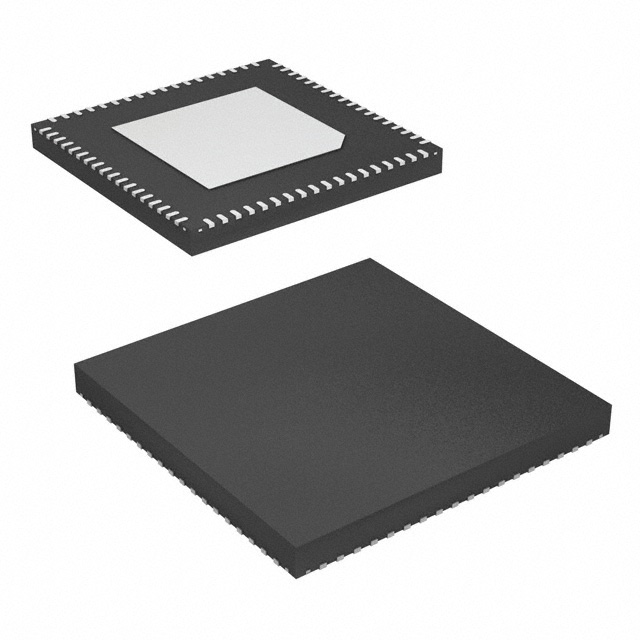
- Part No.:
- 8T49N286A-998NLGI
- Manufacturer:
- Renesas
- Package:
- 72-VFQFN Exposed Pad
- Datasheet:
-
 8T49N286A-998NLGI.pdf
- Description:
- IC TRANSLATOR UNIV FREQ VFQFN
- Quantity:
- Payment:

- Shipping:

Inventory:205
Please send an inquiry. Send us your inquiry, and we will respond immediately.
Product details
Overview
8T49N286A-998NLGI from Renesas Electronics (formerly IDT) is a programmable universal frequency translator IC designed for high-precision clock synthesis and jitter attenuation in telecom, datacom, and enterprise networking systems. It supports up to 4 differential or single-ended inputs and 8 LVPECL/LVDS/LVCMOS outputs, delivers <150 fs RMS jitter (12 kHz–20 MHz), and operates with a 3.3 V core supply and configurable 1.8/2.5/3.3 V output supplies.
For engineers reviewing the 8T49N286A-998NLGI datasheet, 8T49N286A-998NLGI pinout, 8T49N286A-998NLGI application, or 8T49N286A-998NLGI equivalent, key selection considerations include its fractional-N PLL architecture, I²C programmability, EEPROM boot capability, mixed-voltage output support, and compatibility with Timing Commander™ configuration software.
Technical Context
The 8T49N286A-998NLGI implements a dual-loop fractional-N PLL architecture: one loop for input reference clean-up and jitter attenuation, and a second for flexible frequency synthesis. It accepts input frequencies from 0.001 MHz to 750 MHz and generates output frequencies from 0.001 MHz to 1.25 GHz across eight independently configurable outputs.
It features integrated EEPROM for autonomous boot, GPIO-controlled DC settings (CLK_SEL, PLL_BYPASS), and hardware-configurable input termination (AC-coupled differential/single-ended). Output voltage levels (1.8 V/2.5 V/3.3 V) are per-output selectable via dedicated VCCOx rails, enabling mixed-signal timing distribution without level-shifting components.
Key Specifications
| Parameter | Value and Actual Design Meaning |
|---|---|
| Output Count | 8 outputs (Q0–Q7), each configurable as differential pair or two single-ended signals |
| RMS Jitter (12 kHz–20 MHz) | <150 fs - enables compliance with stringent OC-192/SONET, SyncE, and 10G/25G Ethernet timing masks |
| Input Frequency Range | 0.001 MHz to 750 MHz - supports legacy T1/E1, GPS, and high-speed serial references |
| Output Frequency Range | 0.001 MHz to 1.25 GHz - covers PCIe Gen5, DDR5, and 100G KR4 clocking requirements |
| Supply Voltages | VDD = 3.3 V (core); VDDO configurable per output bank at 1.8 V / 2.5 V / 3.3 V - eliminates external level shifters |
| Interface | I²C (up to 400 kHz) + EEPROM boot - enables unattended startup and field reconfiguration without host MCU |
| Package | 64-pin QFN (9 mm × 9 mm, 0.5 mm pitch) - RoHS-compliant, thermally enhanced for high-density timing modules |
Pinout & Package
8T49N286A-998NLGI is housed in a 64-pin QFN package (9 mm × 9 mm, 0.5 mm pitch) with exposed thermal pad. Pin functions are validated per Renesas' official 8T49N286 datasheet and EVK-UFT285-6-7 schematic documentation.
| Pin/Terminal | Circuit Role | Design Meaning |
|---|---|---|
| CLK0, nCLK0 | Differential input pair 0 | AC-coupled, configurable for LVPECL/LVDS/LVCMOS; supports auto-sensing via CLK0_S/nCLK0_S |
| Q0P, Q0N | Differential output pair 0 | Programmable LVPECL/LVDS; terminated internally or externally depending on VCCO0 and resistor network |
| VCCO0–VCCO7 | Output bank power supplies | Each powers one output (Q0–Q7); enables independent voltage selection (1.8/2.5/3.3 V) per output |
| SCL, SDA | I²C interface | Supports configuration and register read/write; compatible with standard 3.3 V I²C masters |
| RESET_N | Active-low asynchronous reset | Hardware-initiated full device reset; synchronous to internal clocks after deassertion |
Key Features
| Feature | Design Value |
|---|---|
| Fractional-N dual-loop PLL | Enables ultra-low-jitter synthesis while rejecting input phase noise - critical for SyncE and PTP boundary clocks |
| EEPROM-based autonomous boot | Loads configuration at power-up without host intervention - essential for headless systems and carrier-grade equipment |
| Mixed-voltage output banks | Eliminates need for discrete level translators when driving heterogeneous interfaces (e.g., 1.8 V FPGA + 3.3 V PHY) |
| Configurable input termination | Single-board support for differential (LVPECL/LVDS) and single-ended (LVCMOS/HCSL) references via jumper-selectable AC coupling |
| GPIO control of key modes | DIP-switch or hardwired control of CLK_SEL and PLL_BYPASS allows factory-mode configuration or fail-safe bypass operation |
Applications
| 5G Radio Unit (RU) | Enterprise Switch Timing Module |
|---|---|
|
Use Scenario: Precise synchronization of multiple RF transceivers and fronthaul interfaces in O-RAN compliant radios. IC Role / Device Role / Timing Role: Jitter-attenuating clock generator providing low-phase-noise 30.72 MHz, 122.88 MHz, and 245.76 MHz clocks to ADC/DACs and eCPRI PHYs. Use Value: Achieves <150 fs RMS jitter, meeting ITU-T G.8262 EEC-2 mask for base station timing and enabling sub-100 ns time alignment. |
Use Scenario: Centralized clock distribution across multi-chip switch ASICs, packet processors, and SerDes lanes in 10/25/100 GbE top-of-rack switches. IC Role / Device Role / Timing Role: Universal frequency translator generating synchronized clocks for PCIe Gen4/5 root complexes, DDR5 memory controllers, and IEEE 1588 timestamp units. Use Value: Eight independent outputs with per-bank voltage control eliminate interposer-level translation, reducing BOM count and board area by ~30% vs. discrete solutions. |
| Optical Transport Terminal | SD-WAN Edge Appliance |
|
Use Scenario: Clock recovery and regeneration in OTN (OTU2/OTU4) line cards requiring SONET/SDH-compliant jitter performance. IC Role / Device Role / Timing Role: Jitter cleaner and synthesizer converting incoming 2.488 GHz or 9.953 GHz OTU clock into multiple lower-rate clocks (e.g., 155.52 MHz, 622.08 MHz). Use Value: Dual-loop architecture suppresses input wander and jitter beyond GR-253-CORE limits, ensuring BER <1e−12 over 100 km fiber links. |
Use Scenario: Multi-WAN aggregation appliance requiring precise time-stamping and deterministic packet scheduling across LTE, xDSL, and fiber interfaces. IC Role / Device Role / Timing Role: Low-jitter clock source for ARM-based SoC timers, hardware timestamp engines, and GNSS-disciplined oscillators. Use Value: EEPROM boot ensures deterministic timing behavior at cold start; I²C reprogrammability enables remote firmware-triggered clock profile updates during service activation. |
Equivalent & Alternatives
The following parts are listed as comparable options for similar universal frequency translator applications.
| Alternative Part | Technical Difference | Application Difference | Selection Advice |
|---|---|---|---|
| Si5341-B-GM | 4-output, higher integration (integrated crystal option), lower max output frequency (800 MHz) | Better suited for compact, cost-sensitive client-side timing; lacks per-output VCCO flexibility | Choose for space-constrained designs where 4 outputs suffice and crystal integration reduces bill-of-materials |
| LMK04832RHAR | 6-output, dual cascaded PLLs, JESD204B-specific features, no EEPROM boot | Optimized for high-speed data converter timing; requires external microcontroller for configuration | Prefer when synchronizing ADCs/DACs in radar or medical imaging systems with JESD204B lane alignment |
Compared with Si5341-B-GM and LMK04832RHAR, the 8T49N286A-998NLGI uniquely balances 8-output scalability, per-bank voltage control, and autonomous EEPROM boot-making it optimal for carrier-class infrastructure where reliability, configurability, and mixed-interface timing coexist.
Availability
8T49N286A-998NLGI is available at Aetrix Electronics and suitable for 5G radio unit timing, optical transport terminal clock regeneration, enterprise switch clock distribution, and SD-WAN edge appliance synchronization requiring stable component supply and long-term lifecycle assurance.
Supply support for 8T49N286A-998NLGI includes scheduled delivery planning, volume procurement assistance, BOM continuity management, traceable sourcing, and lifecycle availability coordination for OEM customers, industrial embedded developers, connected-device designers, and electronics production programs.
Manufacturer
Renesas Electronics Corporation is a global semiconductor leader delivering trusted embedded design innovation, with deep expertise in timing, analog, and connectivity solutions for infrastructure and industrial markets.
The 8T49N286A-998NLGI belongs to Renesas' Universal Frequency Translator (UFT) family - engineered specifically for high-reliability, multi-protocol timing in telecom transport, datacenter switching, and wireless infrastructure equipment.
FAQ
What is the primary function of the 8T49N286A-998NLGI in a timing system?
The 8T49N286A-998NLGI serves as a programmable universal frequency translator that performs both jitter attenuation and precise frequency synthesis. It cleans noisy input references using a dual-loop fractional-N PLL and generates up to eight low-jitter output clocks with independent format and voltage configuration. Its role in a timing system is to provide deterministic, high-stability clocking for sensitive interfaces like SerDes, memory controllers, and RF sampling circuits - all within a single 64-pin QFN package.
Does the 8T49N286A-998NLGI support autonomous startup without a host processor?
Yes, the 8T49N286A-998NLGI supports autonomous startup via on-board EEPROM boot. When configured for EEPROM mode, the device loads its complete register map-including input selection, PLL settings, output formats, and VCCO assignments-at power-up without requiring I²C communication from a host MCU. This feature is validated in the EVK-UFT285-6-7 evaluation board documentation and is essential for carrier-grade systems requiring zero-touch provisioning and fail-safe timing recovery.
Can the 8T49N286A-998NLGI generate different output voltages simultaneously?
Yes, the 8T49N286A-998NLGI supports true mixed-voltage operation: each of its eight outputs (Q0–Q7) connects to an independent VCCOx power rail (VCCO0 through VCCO7), allowing simultaneous 1.8 V, 2.5 V, and 3.3 V LVCMOS outputs on the same device. This is implemented via discrete 0 Ω resistors on the EVK-UFT285-6-7 board, which can be removed to isolate individual VCCOx rails and bias them with separate supplies - eliminating external level shifters in heterogeneous timing architectures.
What input signal types does the 8T49N286A-998NLGI accept?
The 8T49N286A-998NLGI accepts both differential (LVPECL, LVDS, HCSL) and single-ended (LVCMOS) input signals across its four clock inputs (CLK0–CLK3). Input termination is AC-coupled by default, with sense lines (e.g., CLK0_S/nCLK0_S) provided for oscilloscope monitoring. For sub-1 MHz signals, the evaluation board recommends replacing coupling capacitors with zero-ohm resistors and ensuring input DC common-mode voltage meets the device's Vcmr specification - as confirmed in the EVK-UFT285-6-7 User Guide Section 12.
How is the 8T49N286A-998NLGI configured and programmed in-system?
The 8T49N286A-998NLGI is configured via its standard I²C interface (SCL/SDA pins), supporting up to 400 kHz operation. Renesas provides Timing Commander™ software, which communicates with the device through the EVK-UFT285-6-7 USB interface to program registers, store configurations in external EEPROM, and perform real-time jitter measurements. All configuration parameters - including PLL dividers, output formats, slew rates, and power-down states - are accessible through documented register maps in the official 8T49N286 datasheet.
8T49N286A-998NLGI Specifications
- Product attributes
- Attribute value
- Manufacturer:
- Renesas
- Series:
- FemtoClock® NG
- Package/Case:
- 72-VFQFN Exposed Pad
- Packaging:
- Tray
- Product Status:
- Active
- Programmable:
- Not Verified
- Type:
- -
- PLL:
- Yes with Bypass
- Input:
- HCSL, LVCMOS, LVDSM, LVHSTL, LVPECL, Crystal
- Output:
- HSCL, LVCMOS, LVDS, LVPECL
- Number of Circuits:
- 1
- Ratio - Input:Output:
- 5:8
- Differential - Input:Output:
- Yes/Yes
- Frequency - Max:
- 1GHz
- Divider/Multiplier:
- Yes/No
- Voltage - Supply:
- 2.375V ~ 3.465V
- Operating Temperature:
- -40°C ~ 85°C
- Mounting Type:
- Surface Mount
- Grade:
- -
- Qualification:
- -
- Supplier Device Package:
- 72-VFQFPN (10x10)
8T49N286A-998NLGI FAQ
1.How can I place an order for 8T49N286A-998NLGI through Aetrix?
Please submit a Request for Quotation (RFQ) for 8T49N286A-998NLGI on Aetrix. Our sales agent will provide a competitive quotation and guide you through the order confirmation once you accept the terms.
2.Are the price and stock information for 8T49N286A-998NLGI reliable?
The price and inventory of 8T49N286A-998NLGI are updated periodically and may fluctuate due to market conditions. Stock and pricing data are typically refreshed every 24 hours. Quotation validity for 8T49N286A-998NLGI is usually 5 days.
3.What payment methods are accepted for 8T49N286A-998NLGI?
We accept Wire Transfer, PayPal, Credit Card, Western Union, MoneyGram, and Escrow for 8T49N286A-998NLGI transactions.
Note: Certain payment methods may incur a processing fee.
4.How is shipping managed for 8T49N286A-998NLGI?
8T49N286A-998NLGI orders can be shipped via leading logistics carriers, including DHL, UPS, FedEx, TNT, or Registered Mail.
Once your 8T49N286A-998NLGI order is processed, you will receive an email with the shipment details and tracking number.
Note: Tracking information may take up to 24 hours to appear. Express delivery typically takes 3–5 business days.
5.How can I obtain technical support or documentation for 8T49N286A-998NLGI?
For technical support, including 8T49N286A-998NLGI datasheets, pinout diagrams, or application guidance, please contact our engineering support team. They can provide detailed documentation and assistance for your 8T49N286A-998NLGI requirements.
6.How does Aetrix verify that 8T49N286A-998NLGI is sourced from the original manufacturer or authorized distributors?
All 8T49N286A-998NLGI products on Aetrix are procured from qualified distributors and authorized channels. Our dedicated quality assurance team conducts strict verification, including traceability checks and, if necessary, third-party testing. This ensures that 8T49N286A-998NLGI meets industry standards.
7.What is the process for return or replacement of 8T49N286A-998NLGI?
All 8T49N286A-998NLGI units undergo pre-shipment inspection (PSI). If there is an issue with 8T49N286A-998NLGI, returns or replacements are accepted under the following conditions:
1.Quantity discrepancies, incorrect items, or visible external defects (such as breakage or corrosion), acknowledged by Aetrix.
2.The issue is reported within 90 days of delivery.
3.The 8T49N286A-998NLGI part is unused and in its original packaging.
Return procedure for 8T49N286A-998NLGI:
1.Submit a request within 90 days.
2.Obtain a Return Material Authorization (RMA) from Aetrix.
8T49N286A-998NLGI Tags

-
CD74HCT4046AM96
Texas Instruments

-
MC14046BDWR2G
onsemi

-
501MILFT
Renesas
-
CD74HC7046AM
Texas Instruments

-
CDCVF2505PWR
Texas Instruments

-
RC19004A100GNL#KB0
Renesas

-
SI5351A-B-GTR
Skyworks Solutions Inc.

-
CY2305SXI-1T
Infineon Technologies
-
570BILFT
Renesas

-
CDCE913PWR
Texas Instruments
-
CY2305SXI-1HT
Infineon Technologies

-
DS1086LU+T
Analog Devices Inc./Maxim Integrated
Tech Hub

TTL and CMOS logic families differ in thresholds, loading, output drive, power and timing. This engineering guide compares 74HC and 74HCT, calculates noise margins and checks 3.3 V/5 V compatibility.

A practical engineering guide to 3.3V and 5V logic compatibility, input thresholds, resistor dividers, translator ICs, MOSFET level shifting, I2C pull-ups, timing limits and power-sequencing risks.

The 74HC595 uses push-pull logic outputs, while the TPIC6B595 uses 50 V open-drain DMOS sinks for higher-power loads. This guide compares timing, current limits, 3.3 V interfacing, load wiring, thermal…

The 74HC595 converts serial data into eight stable parallel outputs. This guide covers pin functions, shift and storage timing, OE and MR behavior, drive-current limits, cascading, voltage compatibilit…

A technical comparison of level-sensitive latches and edge-triggered flip-flops, covering timing windows, setup and hold limits, master–slave operation, time borrowing, race-through, HDL inference and…

A D latch stores one bit while Enable controls when data can pass. This reference covers gate-level operation, truth tables, transparency, setup and hold timing, LE versus OE, common ICs and practical …

An SR latch stores one bit through cross-coupled feedback. This engineering reference covers NOR and NAND implementations, truth tables, forbidden-state recovery, gated operation, switch debouncing, fa…

Latch circuits retain one bit through feedback. This technical reference covers SR and D latches, truth tables, transparency, timing limits, latch-versus-flip-flop behavior, applications and common log…

An engineering guide to LED driver operation, constant-current and constant-voltage outputs, linear and switching topologies, dimming, IC selection, calculations, replacement compatibility, and fault c…

Operational amplifier guide covering op amp basics, feedback, ideal vs real op amps, common configurations, buffer circuits, offset, bias current, gain-bandwidth, slew rate, rail-to-rail limits and sel…


