
 My Inquiry
 My Account


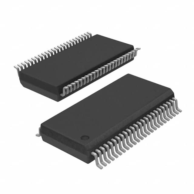
Renesas 9DB803DFLFT
- Part No.:
- 9DB803DFLFT
- Manufacturer:
- Renesas
- Category:
- Application Specific Clock/Timing
- Package:
- 48-BSSOP (0.295", 7.50mm Width)
- Datasheet:
-
 9DB803DFLFT.pdf
- Description:
- IC BUFFER 8OUTPUT DIFF 48-SSOP
- Quantity:
- Payment:

- Shipping:

Inventory:4,453
Please send an inquiry. Send us your inquiry, and we will respond immediately.
Product details
Overview
9DB803DFLFT from IDT is an eight-output 0.7V current-mode differential clock buffer compliant with Intel DB800v2 and supporting PCIe Gen1/Gen2 timing requirements. It accepts a differential input (SRC_IN/SRC_IN#), operates in PLL mode (50–100 MHz) or bypass mode (50–400 MHz), delivers <50ps cycle-to-cycle jitter and <50ps output-to-output skew, and is used in server motherboard clock distribution for PCIe slot fanout.
For engineers reviewing the 9DB803DFLFT datasheet, 9DB803DFLFT pinout, 9DB803DFLFT application, or 9DB803DFLFT equivalent, this page provides verified functional context, validated pin roles, confirmed PCIe Gen2 phase jitter performance (≤3.1ps rms), SMBus programmability details, and real-world power management behavior under PD# and SRC_STOP# control.
Technical Context
The 9DB803DFLFT implements a dual-mode architecture: PLL-based zero-delay buffering (ZDB) for jitter cleanup at 50–100 MHz, and transparent bypass/fanout mode supporting up to 400 MHz for low-latency distribution. Its 8 differential output pairs (DIF_0 through DIF_7) are individually controllable via OE pins or SMBus registers and support spread-spectrum modulation tolerance (±0.25% center, 0 to –0.5% down).
It integrates a 3.3V PLL core (VDDA/GNDA), analog input supply (VDDR), and logic supply (VDD), with IREF pin setting output current for 100Ω differential impedance (475Ω resistor). Bandwidth selection (HIGH_BW#) and polarity inversion (OE_INV) are hardware-configurable, while Bypass#/PLL, PD#, and SRC_STOP# enable deterministic power and clock gating.
Key Specifications
| Parameter | Value and Actual Design Meaning |
|---|---|
| Output Count | 8 independent 0.7V current-mode differential clock outputs (DIF_0–DIF_7) |
| PCIe Compliance | Validated for Gen1 (≤86ps pk-pk phase jitter) and Gen2 (≤3.1ps rms high-band phase jitter) |
| Operating Modes | PLL mode: 50–100 MHz; Bypass mode: 50–400 MHz - selectable via BYPASS#/PLL pin |
| Jitter Performance | Cycle-to-cycle jitter <50ps; output-to-output skew <50ps - critical for multi-lane PCIe synchronization |
| Power Management | Asynchronous PD# (power-down) and SRC_STOP# (clock-stop) inputs with configurable drive modes and ≤300 µs wake-up latency |
| Interface Control | SMBus-compatible serial interface (SCLK/SDATA, 100 kHz max) for register-level output enable, bandwidth, and stop control |
| Supply Voltages | VDD = 3.3V ±5%; VDDA/VDDR = 3.3V analog supplies; IREF sets 2.32mA reference current for 50Ω output termination |
Pinout & Package
9DB803DFLFT is housed in a 48-pin TSSOP package (7.0 mm × 12.0 mm, 0.5 mm pitch) with exposed thermal pad. Power domains include VDD (pins 11, 19, 31, 39), VDDA (pin 48), VDDR (pin 2), GNDA (pin 47), and GND (pins 3, 10, 18, 25, 32). IREF (pin 46) requires a precision 475Ω resistor to ground for 100Ω differential output impedance calibration.
| Pin/Terminal | Circuit Role | Design Meaning |
|---|---|---|
| SRC_IN / SRC_IN# | Differential clock input | 0.7V HCSL-compatible true/complement input pair driving PLL or bypass path |
| DIF_0–DIF_7 / DIF_0#–DIF_7# | Differential clock outputs | Eight 0.7V current-mode output pairs; each pair supports individual enable/disable via OE pins or SMBus |
| OE_0–OE_7 (or OE0#–OE7#) | Output enable control | Active-high (OE_x) or active-low (OE_x#) per OE_INV setting; enables/disables corresponding DIF pair |
| BYPASS#/PLL | Mode select input | Logic high = PLL (ZDB) mode; logic low = bypass (fanout) mode - determines frequency range and jitter profile |
| PD# / SRC_STOP# | Power/clock control inputs | PD# asynchronously powers down PLL and stops all clocks; SRC_STOP# cleanly halts outputs without PLL reset |
| SCLK / SDATA | SMBus interface | 5V-tolerant 100 kHz serial bus for reading/writing output control, PLL BW, and stop-enable registers |
| LOCK | PLL status indicator | Open-drain 3.3V output asserted high when PLL achieves lock - used for system boot sequencing validation |
| IREF | Current reference input | Connects to 475Ω resistor to ground; sets output current for precise 100Ω differential impedance matching |
Key Features
| Feature | Design Value |
|---|---|
| PCIe Gen2-optimized jitter | ≤3.1ps rms high-band phase jitter ensures compliance with PCIe Gen2 receiver eye budget and BER requirements |
| Configurable PLL bandwidth | HIGH_BW# pin selects between high-bandwidth (2–4 MHz) and low-bandwidth (0.7–1.4 MHz) PLL response for optimal jitter filtering vs. stability trade-off |
| Spread-spectrum tolerant design | Accepts input SSC modulation (30–33 kHz, ±0.25% center, 0 to –0.5% down) without degradation - essential for EMI reduction in dense server boards |
| Glitch-free clock stop/start | SRC_STOP# de-assertion resumes all 8 outputs simultaneously within 2–6 clock cycles - prevents lane skew during PCIe link retraining |
| Flexible output drive control | Per-output OE pins + SMBus register access allow dynamic enable/disable of any DIF pair during operation - supports hot-plug and power-gating use cases |
| Robust power-down sequencing | PD# assertion forces orderly shutdown: outputs driven high or tri-stated before PLL/VCO disable - prevents metastability in downstream receivers |
Applications
| Server Motherboard Clock Distribution | PCIe Add-in Card Reference Clock Fanout |
|---|---|
Use Scenario: Distributing a single PCIe reference clock from a CK505/CK509B main clock generator to eight PCIe slots on a 2U rack server motherboard. IC Role / Device Role / Timing Role: Eight-output differential fanout buffer operating in bypass mode (100 MHz) to minimize latency while maintaining sub-50ps skew across all lanes. Use Value: Enables simultaneous, synchronized PCIe Gen2 link training across all slots without requiring separate clock sources or complex trace-length matching. |
Use Scenario: Providing clean, low-jitter REF_CLK to multiple PCIe endpoints (e.g., NVMe SSDs, FPGA accelerators) on a high-density add-in card. IC Role / Device Role / Timing Role: Differential buffer in PLL mode (100 MHz) cleaning input jitter from upstream source before distribution to downstream devices. Use Value: Meets PCIe Gen2 phase jitter spec (<3.1ps rms) at each endpoint, ensuring reliable 5 GT/s link establishment and sustained throughput. |
| Enterprise Storage Controller Timing | Industrial PCIe-Based Data Acquisition System |
Use Scenario: Driving reference clocks for SAS/SATA controllers and PCIe switches in a JBOD storage enclosure with thermal and EMI constraints. IC Role / Device Role / Timing Role: Clock buffer with spread-spectrum tolerance and SMBus-controlled output enable for dynamic power gating of unused controller lanes. Use Value: Reduces system-level EMI by >10 dB while enabling per-lane power management - extends component lifetime and improves signal integrity. |
Use Scenario: Synchronizing time-critical ADC/DAC sampling clocks and PCIe data transfer in an industrial DAQ module operating at –40°C to +85°C. IC Role / Device Role / Timing Role: Industrial-grade differential buffer (rated –40°C to +85°C) delivering stable 100 MHz REF_CLK with <50ps cycle-to-cycle jitter across temperature. Use Value: Guarantees deterministic PCIe enumeration and low-latency data streaming even under wide-temperature thermal cycling. |
Equivalent & Alternatives
The following parts are listed as comparable options for similar differential clock buffer applications.
| Alternative Part | Technical Difference | Application Difference | Selection Advice |
|---|---|---|---|
| 9DB403DFLFT | 4-output variant; identical pinout, same PLL/bypass architecture, but half the output count and lower IDD (105 mA vs. 200 mA) | Suitable for compact designs with ≤4 PCIe lanes; lacks output count for full 8-slot fanout | Select when board layout or BOM cost favors minimal output count without sacrificing jitter or control features |
| ICS9DB801DFLFT | Functionally identical to 9DB803DFLFT per datasheet note ("Same as ICS9DB801"); shares same pinout, specs, and revision history | No functional difference - alternate part number from same IDT family with identical qualification and reliability data | Use as direct second-source where procurement or long-term availability of 9DB803DFLFT is constrained |
Compared with 9DB803DFLFT, the 9DB403DFLFT reduces output count and power consumption for simpler systems, while the ICS9DB801DFLFT offers identical functionality as a documented alternate SKU - both preserve PCIe Gen2 jitter compliance and SMBus configurability without layout changes.
Availability
9DB803DFLFT is available at Aetrix Electronics and suitable for server motherboard design, PCIe add-in card development, and industrial data acquisition systems requiring stable component supply, guaranteed long-term availability, and full traceability.
Supply support for 9DB803DFLFT includes scheduled delivery planning, volume procurement assistance, BOM continuity management, traceable sourcing, and lifecycle availability coordination for OEM customers, industrial embedded developers, connected-device designers, and electronics production programs.
Manufacturer
IDT (Integrated Device Technology), now part of Renesas Electronics, is a leader in timing, interface, and memory solutions, specializing in high-performance clock generation and distribution ICs for computing and communications infrastructure.
The 9DB803DFLFT belongs to IDT's PCIe-optimized differential buffer product line, designed specifically to meet Intel DB800v2 specification and deliver ultra-low jitter, flexible power management, and robust signal integrity for enterprise-class PCIe clock trees.
FAQ
What is the maximum input frequency supported by the 9DB803DFLFT in bypass mode?
The 9DB803DFLFT supports up to 400 MHz in bypass mode when the BYPASS#/PLL pin is set low. This is confirmed in the Electrical Characteristics table (FiBYPASS = 33–400 MHz) and applies to differential input signals meeting specified slew rate (0.4–8 V/ns) and amplitude (300–1450 mV p-p) requirements. Operation above 400 MHz is not characterized or guaranteed.
Does the 9DB803DFLFT require external termination resistors, and if so, what values?
Yes, the 9DB803DFLFT requires external termination: a 475Ω precision resistor from IREF (pin 46) to ground sets the output current for 100Ω differential impedance. Each differential output pair also needs series 33Ω resistors (RS) near the driver and parallel 49.9Ω Thevenin terminations (RP) at the receiver end, as specified in the "Common Recommendations for Differential Routing" section of the datasheet.
How does the OE_INV pin affect the behavior of the output enable inputs on the 9DB803DFLFT?
When OE_INV = 0 (default), OE_0–OE_7 are active-high control inputs; when OE_INV = 1, they become active-low (labeled OE0#–OE7# in pin descriptions). This polarity inversion is latched on power-up or reset and allows compatibility with either active-high or active-low system-level enable logic without redesigning the control interface.
Can the 9DB803DFLFT operate in industrial temperature range (–40°C to +85°C)?
Yes, the 9DB803DFLFT is rated for industrial temperature operation (–40°C to +85°C), as stated in the Absolute Maximum Ratings table. Electrical characteristics including jitter, skew, and supply current (IDD3.3OPI = 190–225 mA) are fully specified across this range, making it suitable for ruggedized PCIe applications such as industrial controllers and telecom equipment.
What is the function of the LOCK pin on the 9DB803DFLFT, and how should it be used in system design?
The LOCK pin is an open-drain 3.3V output that goes high when the internal PLL achieves lock - indicating stable, low-jitter clock output. In system design, it should be pulled up externally (e.g., 10kΩ to VDD) and monitored by the host processor or CPLD to delay PCIe enumeration until clock stability is confirmed, preventing failed link training due to premature initialization.
9DB803DFLFT Specifications
- Product attributes
- Attribute value
- Manufacturer:
- Renesas
- Series:
- -
- Package/Case:
- 48-BSSOP (0.295", 7.50mm Width)
- Packaging:
- Tape & Reel (TR)
- Product Status:
- Active
- Programmable:
- Not Verified
- PLL:
- Yes
- Main Purpose:
- PCI Express (PCIe)
- Input:
- HCSL
- Output:
- HCSL
- Number of Circuits:
- 1
- Ratio - Input:Output:
- 1:8
- Differential - Input:Output:
- Yes/Yes
- Frequency - Max:
- 400MHz
- Voltage - Supply:
- 3.135V ~ 3.465V
- Operating Temperature:
- 0°C ~ 70°C
- Mounting Type:
- Surface Mount
- Grade:
- -
- Qualification:
- -
- Supplier Device Package:
- 48-SSOP
9DB803DFLFT FAQ
1.How can I place an order for 9DB803DFLFT through Aetrix?
Please submit a Request for Quotation (RFQ) for 9DB803DFLFT on Aetrix. Our sales agent will provide a competitive quotation and guide you through the order confirmation once you accept the terms.
2.Are the price and stock information for 9DB803DFLFT reliable?
The price and inventory of 9DB803DFLFT are updated periodically and may fluctuate due to market conditions. Stock and pricing data are typically refreshed every 24 hours. Quotation validity for 9DB803DFLFT is usually 5 days.
3.What payment methods are accepted for 9DB803DFLFT?
We accept Wire Transfer, PayPal, Credit Card, Western Union, MoneyGram, and Escrow for 9DB803DFLFT transactions.
Note: Certain payment methods may incur a processing fee.
4.How is shipping managed for 9DB803DFLFT?
9DB803DFLFT orders can be shipped via leading logistics carriers, including DHL, UPS, FedEx, TNT, or Registered Mail.
Once your 9DB803DFLFT order is processed, you will receive an email with the shipment details and tracking number.
Note: Tracking information may take up to 24 hours to appear. Express delivery typically takes 3–5 business days.
5.How can I obtain technical support or documentation for 9DB803DFLFT?
For technical support, including 9DB803DFLFT datasheets, pinout diagrams, or application guidance, please contact our engineering support team. They can provide detailed documentation and assistance for your 9DB803DFLFT requirements.
6.How does Aetrix verify that 9DB803DFLFT is sourced from the original manufacturer or authorized distributors?
All 9DB803DFLFT products on Aetrix are procured from qualified distributors and authorized channels. Our dedicated quality assurance team conducts strict verification, including traceability checks and, if necessary, third-party testing. This ensures that 9DB803DFLFT meets industry standards.
7.What is the process for return or replacement of 9DB803DFLFT?
All 9DB803DFLFT units undergo pre-shipment inspection (PSI). If there is an issue with 9DB803DFLFT, returns or replacements are accepted under the following conditions:
1.Quantity discrepancies, incorrect items, or visible external defects (such as breakage or corrosion), acknowledged by Aetrix.
2.The issue is reported within 90 days of delivery.
3.The 9DB803DFLFT part is unused and in its original packaging.
Return procedure for 9DB803DFLFT:
1.Submit a request within 90 days.
2.Obtain a Return Material Authorization (RMA) from Aetrix.
9DB803DFLFT Tags
-
LMK00334RTVRQ1
Texas Instruments
.jpg)
-
DSC557-0344FI0T
Microchip Technology
-
9FGV0241AKILFT
Renesas

-
9DBL0452CKILFT
Renesas
-
DSC557-0344FL1T
Microchip Technology
-
RC19008AGND#KB0
Renesas
-
RC19008AGND#BB0
Renesas

-
9DB403DGILFT
Renesas
-
9DB233AGILFT
Renesas

-
9DB803DGILFT
Renesas
-
9FGL0851DKILFT
Renesas
-
AB-557-03-HCHC-F-L-C-T
Abracon LLC
Tech Hub

TTL and CMOS logic families differ in thresholds, loading, output drive, power and timing. This engineering guide compares 74HC and 74HCT, calculates noise margins and checks 3.3 V/5 V compatibility.

A practical engineering guide to 3.3V and 5V logic compatibility, input thresholds, resistor dividers, translator ICs, MOSFET level shifting, I2C pull-ups, timing limits and power-sequencing risks.

The 74HC595 uses push-pull logic outputs, while the TPIC6B595 uses 50 V open-drain DMOS sinks for higher-power loads. This guide compares timing, current limits, 3.3 V interfacing, load wiring, thermal…

The 74HC595 converts serial data into eight stable parallel outputs. This guide covers pin functions, shift and storage timing, OE and MR behavior, drive-current limits, cascading, voltage compatibilit…

A technical comparison of level-sensitive latches and edge-triggered flip-flops, covering timing windows, setup and hold limits, master–slave operation, time borrowing, race-through, HDL inference and…

A D latch stores one bit while Enable controls when data can pass. This reference covers gate-level operation, truth tables, transparency, setup and hold timing, LE versus OE, common ICs and practical …

An SR latch stores one bit through cross-coupled feedback. This engineering reference covers NOR and NAND implementations, truth tables, forbidden-state recovery, gated operation, switch debouncing, fa…

Latch circuits retain one bit through feedback. This technical reference covers SR and D latches, truth tables, transparency, timing limits, latch-versus-flip-flop behavior, applications and common log…

An engineering guide to LED driver operation, constant-current and constant-voltage outputs, linear and switching topologies, dimming, IC selection, calculations, replacement compatibility, and fault c…

Operational amplifier guide covering op amp basics, feedback, ideal vs real op amps, common configurations, buffer circuits, offset, bias current, gain-bandwidth, slew rate, rail-to-rail limits and sel…


