
 My Inquiry
 My Account


Renesas 9DBV0531AKLFT
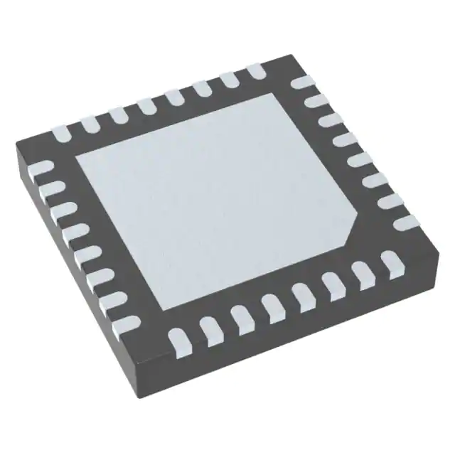
- Part No.:
- 9DBV0531AKLFT
- Manufacturer:
- Renesas
- Category:
- Specialized
- Package:
- 32-VFQFN Exposed Pad
- Datasheet:
-
 9DBV0531AKLFT.pdf
- Description:
- VFQFPN 5.00X5.00X0.90 MM, 0.50MM
- Quantity:
- Payment:

- Shipping:

Inventory:1,510
Please send an inquiry. Send us your inquiry, and we will respond immediately.
Product details
Overview
9DBV0531AKLFT from Renesas Electronics is a 5-output, 1.8V low-power PCIe Gen5 fanout buffer with LP-HCSL outputs, 33Ω termination, OE# control per output, and SMBus-configurable slew rate and amplitude. It delivers <40fs RMS additive phase jitter in Common Clocked architecture and supports 1–200MHz input frequencies for high-speed server clock distribution.
For engineers reviewing the 9DBV0531AKLFT datasheet, 9DBV0531AKLFT pinout, 9DBV0531AKLFT application, or 9DBV0531AKLFT equivalent, this device is selected for PCIe Gen5-compliant timing in space-constrained 5×5 mm VFQFPN layouts where output enable granularity, spread-spectrum compatibility, and ultra-low additive jitter are critical design requirements.
Technical Context
The 9DBV0531AKLFT implements a zero-delay fanout architecture with differential HCSL outputs, no internal PLL, and direct clock replication from CLK_IN/CLK_IN#. Its 33Ω integrated output impedance eliminates external series resistors for both 85Ω and 100Ω PCB trace systems.
It features an SMBus interface with three selectable addresses (via vSADR_tri), 3.3V-tolerant SCLK/SDATA pins, and factory-default operation-no SMBus configuration required for basic functionality. Power management includes CKPWRGD_PD#-controlled power-down mode with sub-1μA total IDDOPD.
Key Specifications
| Parameter | Value and Actual Design Meaning |
|---|---|
| Outputs | 5 LP-HCSL differential outputs with individual OE# control |
| PCIe Gen5 Additive Jitter | <40fs RMS (Common Clocked architecture, 12kHz–20MHz) |
| Output-to-Output Skew | <50ps (ensures tight timing alignment across all 5 outputs) |
| Operating Frequency | 1MHz to 200MHz (supports PCIe Gen1–Gen5 reference clocks) |
| Power Consumption | 41mW typical at 100MHz (enables thermal efficiency in dense server boards) |
| Package | 32-pin VFQFPN, 5×5 mm, 0.5mm pitch (EPAD grounded) |
| Supply Voltages | VDDDIG1.8 = 1.7–1.9V; VDDO1.8 = 1.7–1.9V; VDDR1.8 = 1.7–1.9V |
Pinout & Package
32-pin Very Thin Quad Flat No-Lead (VFQFPN) package, 5×5 mm body, 0.5 mm pitch, exposed thermal pad (EPAD) connected to GND. Pin 1 is vSADR_tri (tri-level SMBus address select); pin 31 is ^CKPWRGD_PD# (power-down control with internal 120kΩ pull-up).
| Pin/Terminal | Circuit Role | Design Meaning |
|---|---|---|
| vSADR_tri | SMBus address select input | Tri-level latch (GND/VDD/NC) sets one of three SMBus addresses; internal 120kΩ pull-down |
| ^CKPWRGD_PD# | Power-down control input | Low asserts power-down mode; internal 120kΩ pull-up ensures default active state |
| CLK_IN / CLK_IN# | Differential reference clock inputs | True/complementary LVDS/HCSL-compatible inputs; 300mV min swing, 150–900mV crossover voltage |
| DIF0–DIF4 / DIF0#–DIF4# | LP-HCSL differential outputs | 33Ω source-terminated outputs; eliminate 2 external resistors per pair in 85Ω/100Ω systems |
| vOE0#–vOE4# | Individual output enable inputs | Active-low control per output; internal 120kΩ pull-down enables default disable on power-up |
| VDDDIG1.8 / VDDO1.8 / VDDR1.8 | Separate 1.8V supplies | Isolated digital core, output, and analog receiver rails reduce noise coupling and improve jitter performance |
Key Features
| Feature | Design Value |
|---|---|
| Integrated 33Ω LP-HCSL outputs | Eliminates 2 external resistors per output pair, reducing BOM count and layout area in PCIe Gen5 designs |
| SMBus-selectable slew rate & amplitude | Per-output optimization for signal integrity across varying trace lengths and loading without hardware change |
| PCIe CLKREQ# support via OE# pins | Direct hardware-level power gating of individual outputs aligns with PCIe L1 substates for dynamic power savings |
| Factory-default operation | No SMBus initialization required; device functions immediately after power-up and clock stabilization |
| Spread-spectrum compatible | Supports SRIS/SRNS architectures up to 66kHz modulation frequency without degrading additive jitter |
Applications
| Server Clock Distribution | nVME Storage Controller Timing |
|---|---|
Use Scenario: Distributing 100MHz PCIe reference clock to multiple CPU, GPU, and I/O die in dual-socket servers. IC Role / Device Role / Timing Role: Fanout buffer replicating low-jitter clock with per-output enable for dynamic power gating. Use Value: Sub-40fs RMS additive jitter preserves PCIe Gen5 eye margin; 5-output count matches typical CPU socket fanout demand. |
Use Scenario: Providing synchronized 156.25MHz clock to NVMe SSD controller and multiple NAND flash channels. IC Role / Device Role / Timing Role: Low-skew (<50ps) clock fanout enabling deterministic inter-channel timing in high-throughput storage. Use Value: Output-to-output skew ≤50ps prevents setup/hold violations across parallel NAND interfaces. |
| AI Accelerator Board Clocking | Industrial PCIe Backplane Timing |
Use Scenario: Driving clock inputs of multiple FPGA-based AI accelerators sharing a common PCIe root complex. IC Role / Device Role / Timing Role: SMBus-configurable slew rate adapts to diverse FPGA input thresholds and board stack-ups. Use Value: Configurable output amplitude and slew rate reduce EMI and improve signal integrity across heterogeneous loads. |
Use Scenario: Generating robust 125MHz clock for industrial PCIe switch and endpoint cards in extended temperature environments. IC Role / Device Role / Timing Role: Industrial-grade (-40°C to +85°C) fanout buffer with stable 1.8V supply operation. Use Value: Guaranteed operation over full industrial temperature range with <165fs RMS additive jitter at 156.25MHz. |
Equivalent & Alternatives
The following parts are listed as comparable options for similar PCIe fanout buffer applications.
| Alternative Part | Technical Difference | Application Difference | Selection Advice |
|---|---|---|---|
| IDT8T49N242A | 8-output, 1.8V LP-HCSL; higher power (75mW typ); requires external 33Ω resistors | Higher channel count but larger 6×6 mm 48-VFQFPN package; no integrated 33Ω termination | Select when >5 outputs needed and board layout allows larger footprint and extra resistors |
| Si53306-A-GM | 6-output, 1.8V LVDS/LP-HCSL; 1.2V core; SMBus-only configuration (no default operation) | LVDS-compatible outputs; lacks OE# per output; requires SMBus init before use | Select when LVDS interface compatibility is required and firmware-controlled initialization is acceptable |
Compared with IDT8T49N242A and Si53306-A-GM, the 9DBV0531AKLFT offers the smallest footprint (5×5 mm), lowest power (41mW), integrated 33Ω termination, and true plug-and-play operation-making it optimal for space- and power-constrained PCIe Gen5 server and accelerator designs.
Availability
9DBV0531AKLFT is available at Aetrix Electronics and suitable for servers, nVME storage controllers, AI accelerators, and industrial PCIe backplanes requiring stable component supply, long-term lifecycle support, and guaranteed PCIe Gen5 timing compliance.
Supply support for 9DBV0531AKLFT includes scheduled delivery planning, volume procurement assistance, BOM continuity management, traceable sourcing, and lifecycle availability coordination for OEM customers, industrial embedded developers, connected-device designers, and electronics production programs.
Manufacturer
Renesas Electronics is a global semiconductor leader delivering high-performance analog, mixed-signal, and embedded processing solutions for automotive, industrial, infrastructure, and datacenter markets.
The 9DBV0531AKLFT belongs to Renesas' Full Featured PCIe family of fanout buffers, engineered specifically for low-additive-jitter, low-power, and high-density PCIe Gen1–Gen5 clock distribution in next-generation computing platforms.
FAQ
What is the operating temperature range for the 9DBV0531AKLFT?
The 9DBV0531AKLFT is rated for industrial operation from –40°C to +85°C. This range is validated across all electrical specifications including additive phase jitter, output skew, and supply current, ensuring reliable PCIe Gen5 timing performance in demanding server and embedded environments where ambient temperatures exceed commercial limits.
Does the 9DBV0531AKLFT require SMBus configuration to function?
No-the 9DBV0531AKLFT operates with factory-default settings immediately after power-up and clock stabilization. SMBus is optional and used only to modify slew rate, output amplitude, or address; the 9DBV0531AKLFT delivers full LP-HCSL output functionality without any SMBus interaction.
How does the 9DBV0531AKLFT support PCIe CLKREQ# functionality?
The 9DBV0531AKLFT supports PCIe CLKREQ# via its five dedicated vOE0#–vOE4# pins. Each is an active-low, internally pulled-down input that directly gates its corresponding DIFx/DIFx# output pair-enabling hardware-coordinated clock gating aligned with PCIe L1 substate transitions without software intervention.
What is the significance of the 33Ω output impedance in the 9DBV0531AKLFT?
The 33Ω source-terminated LP-HCSL outputs in the 9DBV0531AKLFT eliminate two external 33Ω series resistors per differential pair, reducing BOM cost, PCB area, and signal path discontinuities. This design supports both 85Ω and 100Ω differential trace impedances, simplifying layout for mixed-impedance PCIe Gen5 systems.
Can the 9DBV0531AKLFT be used in SRIS (Separate Reference Independent Spread Spectrum) architectures?
Yes-the 9DBV0531AKLFT is explicitly characterized for SRIS operation, delivering 0.036–0.059ps RMS additive jitter at PCIe Gen5 (32 GT/s) in SRIS mode. Its SMBus-configurable features and wide 1–200MHz input range make it suitable for both SRIS and Common Clocked PCIe clocking topologies.
9DBV0531AKLFT Specifications
- Product attributes
- Attribute value
- Manufacturer:
- Renesas
- Series:
- -
- Package/Case:
- 32-VFQFN Exposed Pad
- Packaging:
- Tape & Reel (TR)
- Product Status:
- Active
- Applications:
- Networking
- Interface:
- SMBus
- Voltage - Supply:
- 1.7V ~ 1.9V
- Supplier Device Package:
- 32-VFQFPN (5x5)
- Grade:
- -
- Qualification:
- -
- Mounting Type:
- Surface Mount
9DBV0531AKLFT FAQ
1.How can I place an order for 9DBV0531AKLFT through Aetrix?
Please submit a Request for Quotation (RFQ) for 9DBV0531AKLFT on Aetrix. Our sales agent will provide a competitive quotation and guide you through the order confirmation once you accept the terms.
2.Are the price and stock information for 9DBV0531AKLFT reliable?
The price and inventory of 9DBV0531AKLFT are updated periodically and may fluctuate due to market conditions. Stock and pricing data are typically refreshed every 24 hours. Quotation validity for 9DBV0531AKLFT is usually 5 days.
3.What payment methods are accepted for 9DBV0531AKLFT?
We accept Wire Transfer, PayPal, Credit Card, Western Union, MoneyGram, and Escrow for 9DBV0531AKLFT transactions.
Note: Certain payment methods may incur a processing fee.
4.How is shipping managed for 9DBV0531AKLFT?
9DBV0531AKLFT orders can be shipped via leading logistics carriers, including DHL, UPS, FedEx, TNT, or Registered Mail.
Once your 9DBV0531AKLFT order is processed, you will receive an email with the shipment details and tracking number.
Note: Tracking information may take up to 24 hours to appear. Express delivery typically takes 3–5 business days.
5.How can I obtain technical support or documentation for 9DBV0531AKLFT?
For technical support, including 9DBV0531AKLFT datasheets, pinout diagrams, or application guidance, please contact our engineering support team. They can provide detailed documentation and assistance for your 9DBV0531AKLFT requirements.
6.How does Aetrix verify that 9DBV0531AKLFT is sourced from the original manufacturer or authorized distributors?
All 9DBV0531AKLFT products on Aetrix are procured from qualified distributors and authorized channels. Our dedicated quality assurance team conducts strict verification, including traceability checks and, if necessary, third-party testing. This ensures that 9DBV0531AKLFT meets industry standards.
7.What is the process for return or replacement of 9DBV0531AKLFT?
All 9DBV0531AKLFT units undergo pre-shipment inspection (PSI). If there is an issue with 9DBV0531AKLFT, returns or replacements are accepted under the following conditions:
1.Quantity discrepancies, incorrect items, or visible external defects (such as breakage or corrosion), acknowledged by Aetrix.
2.The issue is reported within 90 days of delivery.
3.The 9DBV0531AKLFT part is unused and in its original packaging.
Return procedure for 9DBV0531AKLFT:
1.Submit a request within 90 days.
2.Obtain a Return Material Authorization (RMA) from Aetrix.
9DBV0531AKLFT Tags

-
NVT4857UKAZ
NXP Semiconductors

-
TCA8418RTWR
Texas Instruments

-
PCA9546APWR
Texas Instruments

-
MD0100N8-G
Microchip Technology

-
PCA9548APW,118
NXP Semiconductors

-
PCA9540BDP,118
NXP Semiconductors

-
PCA9548APWR
Texas Instruments

-
PCA9546APW,118
NXP Semiconductors

-
PTN3360DBS,518
NXP Semiconductors

-
PCA9546ABS,118
NXP Semiconductors

-
PCA9518PWR
Texas Instruments

-
PCA9545APW,118
NXP Semiconductors
Tech Hub

TTL and CMOS logic families differ in thresholds, loading, output drive, power and timing. This engineering guide compares 74HC and 74HCT, calculates noise margins and checks 3.3 V/5 V compatibility.

A practical engineering guide to 3.3V and 5V logic compatibility, input thresholds, resistor dividers, translator ICs, MOSFET level shifting, I2C pull-ups, timing limits and power-sequencing risks.

The 74HC595 uses push-pull logic outputs, while the TPIC6B595 uses 50 V open-drain DMOS sinks for higher-power loads. This guide compares timing, current limits, 3.3 V interfacing, load wiring, thermal…

The 74HC595 converts serial data into eight stable parallel outputs. This guide covers pin functions, shift and storage timing, OE and MR behavior, drive-current limits, cascading, voltage compatibilit…

A technical comparison of level-sensitive latches and edge-triggered flip-flops, covering timing windows, setup and hold limits, master–slave operation, time borrowing, race-through, HDL inference and…

A D latch stores one bit while Enable controls when data can pass. This reference covers gate-level operation, truth tables, transparency, setup and hold timing, LE versus OE, common ICs and practical …

An SR latch stores one bit through cross-coupled feedback. This engineering reference covers NOR and NAND implementations, truth tables, forbidden-state recovery, gated operation, switch debouncing, fa…

Latch circuits retain one bit through feedback. This technical reference covers SR and D latches, truth tables, transparency, timing limits, latch-versus-flip-flop behavior, applications and common log…

An engineering guide to LED driver operation, constant-current and constant-voltage outputs, linear and switching topologies, dimming, IC selection, calculations, replacement compatibility, and fault c…

Operational amplifier guide covering op amp basics, feedback, ideal vs real op amps, common configurations, buffer circuits, offset, bias current, gain-bandwidth, slew rate, rail-to-rail limits and sel…


