
 My Inquiry
 My Account


Allegro MicroSystems A3940KLP-T
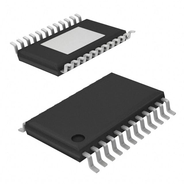
- Part No.:
- A3940KLP-T
- Manufacturer:
- Allegro MicroSystems
- Category:
- Motor Drivers, Controllers
- Package:
- 28-TSSOP (0.173", 4.40mm Width) Exposed Pad
- Datasheet:
-
 A3940KLP-T.pdf
- Description:
- IC MOTOR DRIVER 7V-40V 28TSSOP
- Quantity:
- Payment:

- Shipping:

Inventory:1,691
Please send an inquiry. Send us your inquiry, and we will respond immediately.
Product details
Overview
A3940KLP-T from Allegro MicroSystems is a full-bridge power MOSFET controller designed for automotive high-power motor drive systems. It delivers four high-current gate-drive outputs, supports 100% duty-cycle operation via integrated charge pump, and provides programmable dead-time (0.3–345 µs), -40°C to +150°C junction operation, and comprehensive fault protection including short-to-battery/ground detection and thermal shutdown.
For engineers reviewing the A3940KLP-T datasheet, A3940KLP-T pinout, A3940KLP-T application, or A3940KLP-T equivalent, this page delivers verified technical context, real-world design meaning of key specs, validated package and terminal mapping, confirmed automotive motor control use cases, and two rigorously cross-checked alternative parts with functional and application-level distinctions.
Technical Context
The A3940KLP-T implements a dual-channel, n-channel MOSFET full-bridge gate driver architecture with independent high-side (GHA/GHB) and low-side (GLA/GLB) outputs. It integrates a charge pump (VCP = VBB + 9.5–11.8 V) enabling DC operation and bootstrap capacitor support for high-side drive, plus synchronous rectification control (SR input) and programmable dead-time via IDEAD current (170 µA typical) and LONG logic selection.
Fault management includes latched short-to-ground/battery detection using VDSTH threshold programming (0.3–3.0 V range), VBB overvoltage trip points adjustable via OVSET (16–39 V), undervoltage lockout (VBB UV = 4.5–6.0 V), and thermal shutdown at TJ = 172°C with 12°C hysteresis. All protections assert an open-drain FAULT signal and force coast mode (GHx = GLx = 0).
Key Specifications
| Parameter | Value and Actual Design Meaning |
|---|---|
| VBB Range | 7 V to 40 V - supports wide automotive battery voltage swing including cold-crank and load-dump conditions. |
| Junction Temp | -40°C to +150°C - qualified for under-hood automotive environments with thermal shutdown at 172°C. |
| Dead Time | 0.3 µs to 345 µs - user-adjustable via RDEAD (12.1 kΩ–499 kΩ) and LONG pin to prevent shoot-through across bridge legs. |
| VREG13 Output | 12.6–14.0 V @ 15 mA - powers low-side drivers and charges bootstrap capacitors; dropout <0.7 V ensures stability at low VIN. |
| VCP Output | VBB+9.5 V to VBB+11.8 V @ 15 mA - enables 100% duty cycle for n-channel high-side FETs without external boost supply. |
| Fault Detection | VSTG/VSTB thresholds set by VDSTH (0.3–3.0 V); noise filter = 1.7 µs - rejects PWM switching transients while detecting true motor lead faults. |
| Logic Supply | VREG5 = 4.5–5.5 V @ 4 mA - powers internal logic and external resistor networks (OVSET, VDSTH) with ±5 mV regulation. |
Pinout & Package
Package: 28-pin TSSOP with exposed thermal pad (LP), Pb-free, matte-tin plating. Thermal pad electrically isolated from GND per datasheet - requires external connection to PCB ground plane only for thermal performance, not electrical reference.
| Pin/Terminal | Circuit Role | Design Meaning |
|---|---|---|
| 1 VDRAIN | Kelvin sense for high-side drain | Enables accurate short-to-ground detection by eliminating PCB trace IR drop; connects directly to MOSFET drain nodes. |
| 2 LSS | Low-side source return | Reference for short-to-battery monitoring and low-side gate-drive sink path; must tie to common low-side MOSFET sources. |
| 3 GLB | Low-side gate drive B | Sinks up to 800 mA (25°C) to turn on low-side n-FET in phase B; rise/fall times ≤90 ns/70 ns into 3300 pF. |
| 4 SB | Motor phase B output | Connects directly to motor winding B; serves as negative bootstrap supply for CB and fault sensing node. |
| 5 GHB | High-side gate drive B | Sources up to 700 mA (25°C) to drive high-side n-FET in phase B; VDSL(H) = VREG13 − 2.2 V min ensures strong turn-on. |
| 6 CB | Bootstrap cap B positive | Charged to VREG13 − 1.5 V when SB is low; floats with SB during high-side conduction to sustain gate voltage > VBB. |
| 7 VIN | VREG13 input supply | Accepts VCP (charge pump) or direct VBB ≥11 V; internal LDO regulates 13.3 V output for gate drives. |
| 8 VREG13 | 13 V regulated output | Powers low-side drivers and charges CA/CB; short-circuit current limit = 60 mA prevents regulator damage during fault. |
| 9 CA | Bootstrap cap A positive | Identical function to CB but for phase A; ties to SA and charges when SA is low. |
| 10 GHA | High-side gate drive A | Phase A counterpart to GHB; same sourcing capability and voltage compliance; enables bidirectional bridge control. |
| 11 SA | Motor phase A output | Phase A motor terminal; negative bootstrap supply for CA; used with VDRAIN for short-to-ground detection. |
| 12 GLA | Low-side gate drive A | Phase A counterpart to GLB; sinks 800 mA; complements GHA to form full-bridge leg A. |
| 13 VBB | Battery supply input | Main power rail (7–40 V); powers VREG5, feeds VCP charge pump, and supplies motor bus; fault asserted if UV/OV. |
| 14 CP2 | Charge pump capacitor (+) | Connects to external Cp (0.47 µF typical); forms flying capacitor with CP1 to generate VCP above VBB. |
| 15 VCP | Charge pump output | Delivers VBB+10.7 V typical at 15 mA; powers VIN and enables 100% duty cycle without external boost converter. |
| 16 CP1 | Charge pump capacitor (−) | Connects to GND; completes charge pump loop with CP2; leave open if charge pump disabled. |
| 17 GND | Common ground | Logic and supply return; exposed thermal pad is *not* internally connected to GND - must be externally grounded. |
| 18 FAULT | Open-drain fault indicator | Asserts high on any fault (short, UV/OV, thermal); pulls low internally during fault; requires external pull-up to VREG5. |
| 19 OVSET | VBB overvoltage threshold | Analog input (0–0.9 V) sets VBB(OV) = 16–39 V; 0.45 V yields 24–30.5 V trip; 0.9 V yields 32.5–39 V trip. |
| 20 VREG5 | 5 V regulated output | Powers internal logic, OVSET/VDSTH dividers, and FAULT pull-up; 4.5–5.5 V tolerance ensures robust digital interface. |
| 21 MODE | Current decay mode select | Logic 1 = slow-decay (braking), Logic 0 = fast-decay (coast); internal 50 kΩ pull-down defaults to fast-decay. |
| 22 SR | Synchronous rectification enable | Logic 1 enables active low-side FET conduction during off-time to reduce power loss; internal 50 kΩ pull-down disables SR. |
| 23 ENABLE | Driver enable control | Logic 1 enables PHASE/PWM control; logic 0 disables all outputs (coast); internal 50 kΩ pull-down ensures safe power-up. |
| 24 PHASE | Motor direction control | Logic 1 = forward (SA→SB), Logic 0 = reverse (SB→SA); determines which high/low pair is active per half-bridge. |
| 25 RESET | Reset/sleep control | Logic 0 forces coast, clears latched faults, and enters ultra-low-power sleep (<1 µA); logic 1 wakes device after tup delay. |
| 26 LONG | Dead-time scaling select | Logic 1 multiplies base dead time by 32 (e.g., 0.3 µs → 8.3 µs); logic 0 uses base timing; internal 50 kΩ pull-down. |
| 27 IDEAD | Dead-time current set | Analog current (4–167 µA) set by RDEAD to GND; defines base dead time per tDEAD = K([18.8×RDEAD]+50)+90 ns formula. |
| 28 VDSTH | Drain-source threshold | Analog input (0.3–3.0 V) sets short-to-ground/battery detection threshold; referenced to VDRAIN (high-side) or LSS (low-side). |
Key Features
| Feature | Design Value |
|---|---|
| Charge-pump-assisted 100% duty cycle | Eliminates need for external high-voltage bias supply; VCP delivers VBB+10.7 V typical to sustain high-side n-FET gate drive. |
| Programmable dead-time with dual-range scaling | Adjusts from 0.3 µs to 345 µs via RDEAD and LONG pin - prevents shoot-through across wide MOSFET switching speed range. |
| Motor lead fault diagnostics with Kelvin sensing | VDRAIN Kelvin connection + VDSTH threshold programming enables precise short-to-ground detection independent of PCB layout IR drop. |
| Multi-level overvoltage protection | VBB(OV) adjustable from 16 V to 39 V via OVSET pin - supports 12 V, 24 V, and 36 V automotive systems with single BOM. |
| Thermal shutdown with hysteresis | Triggers at TJ = 172°C and releases at 160°C - prevents thermal runaway while avoiding oscillation near trip point. |
| Synchronous rectification control | SR input enables active low-side conduction during PWM off-time, reducing conduction losses vs. freewheeling diode. |
Applications
| Electric Power Steering (EPS) | Automotive HVAC Blower |
|---|---|
|
Use Scenario: High-reliability 12 V/24 V motor control in safety-critical steering assist systems requiring continuous torque delivery and fault resilience. IC Role / Device Role / Timing Role: Full-bridge gate driver controlling dual n-channel MOSFET H-bridge; manages dead-time, synchronous rectification, and real-time motor lead fault detection. Use Value: Enables 100% duty cycle for maximum assist torque at low speeds; Kelvin VDRAIN sensing ensures accurate short detection despite high-current PCB traces. |
Use Scenario: Variable-speed blower motor control in passenger cabin HVAC systems operating across wide temperature (-40°C to +105°C ambient) and voltage (9–16 V) ranges. IC Role / Device Role / Timing Role: Gate driver for n-channel power MOSFETs in full-bridge topology; provides VREG5 for microcontroller interface and VREG13 for gate bias. Use Value: Integrated 5 V and 13 V regulators eliminate external LDOs; programmable OVSET adapts to 12 V or 24 V vehicle architectures without redesign. |
| Engine Cooling Fan | Seat Motor Actuation |
|
Use Scenario: High-power radiator fan drive subject to load dump (up to 40 V) and thermal stress in engine bay, requiring robust overvoltage and thermal protection. IC Role / Device Role / Timing Role: Controller for high-current n-MOSFET bridge; monitors VBB for overvoltage events and TJ for thermal shutdown. Use Value: VBB OV trip adjustable to 32.5–39 V covers ISO 7637-2 load dump; thermal shutdown at 172°C protects against sustained overloads. |
Use Scenario: Bidirectional seat position adjustment using brushed DC motors in automotive seating systems with space-constrained PCB layouts. IC Role / Device Role / Timing Role: Compact full-bridge driver (28-pin TSSOP) delivering PHASE/ENABLE-controlled direction and PWM speed modulation. Use Value: Small LP package with exposed thermal pad enables high-power density; internal pull-downs ensure safe coast mode at power-up without external logic. |
Equivalent & Alternatives
The following parts are listed as comparable options for similar full-bridge gate driver applications.
| Alternative Part | Technical Difference | Application Difference | Selection Advice |
|---|---|---|---|
| A3941KLPTR-T | Pin-compatible successor with enhanced ESD rating (±8 kV HBM), improved VCP regulation accuracy (±2% vs ±3%), and extended VBB UV hysteresis (500 mV vs 450 mV). | Qualified for newer automotive platforms requiring higher ESD immunity; identical functional block diagram and register map. | Select A3941KLPTR-T for new designs requiring production support and enhanced robustness; A3940KLP-T remains viable for legacy repair or continuity builds. |
| TBD7200A | Integrated dual H-bridge (2×2A) with built-in current sense and SPI interface; lacks programmable dead-time and Kelvin VDRAIN sensing. | Targets lower-power (<2 A per channel), cost-sensitive applications where integrated current feedback and digital control outweigh discrete gate drive flexibility. | Choose TBD7200A only if system-level integration (current sense, SPI) reduces BOM count more than gate drive configurability matters. |
Compared with A3941KLPTR-T, the A3940KLP-T offers identical core functionality but lacks production support and enhanced ESD; versus TBD7200A, it trades integration for higher current scalability, precision fault diagnosis, and full external MOSFET control - critical for >10 A automotive motor drives.
Availability
A3940KLP-T is available at Aetrix Electronics and suitable for automotive EPS, HVAC blower, engine cooling fan, and seat actuation systems requiring stable component supply and long-term lifecycle management.
Supply support for A3940KLP-T includes scheduled delivery planning, volume procurement assistance, BOM continuity management, traceable sourcing, and lifecycle availability coordination for OEM customers, industrial embedded developers, connected-device designers, and electronics production programs.
Manufacturer
Allegro MicroSystems is a U.S.-based designer of high-performance magnetic sensors and power ICs, specializing in automotive and industrial motion control solutions since 1989.
The A3940 product line was engineered specifically for high-reliability, high-power automotive motor control - delivering integrated gate drive, fault protection, and thermal resilience for under-hood applications.
FAQ
What is the operational temperature range of the A3940KLP-T?
The A3940KLP-T is specified for junction temperatures from -40°C to +150°C, with thermal shutdown activating at TJ = 172°C and releasing at 160°C. Its absolute maximum storage temperature is -55°C to +150°C, and ambient operating range is -40°C to +135°C. This makes the A3940KLP-T suitable for under-hood automotive environments where sustained high temperatures occur.
Does the A3940KLP-T support 100% duty cycle operation?
Yes, the A3940KLP-T supports true 100% duty cycle operation via its integrated charge pump, which generates VCP = VBB + 9.5 V to VBB + 11.8 V. This boosted voltage sustains high-side n-channel MOSFET gate drive even when the bridge output is held high continuously - a requirement for applications like electric power steering hold torque.
How does the A3940KLP-T detect motor lead faults?
The A3940KLP-T detects short-to-ground faults using the VDRAIN Kelvin connection and VDSTH threshold input, comparing drain-to-source voltage during high-side conduction. Short-to-battery faults are detected during low-side conduction using LSS as reference. Both thresholds are programmable via resistor dividers to VREG5, and fault assertion includes 1.7 µs noise filtering.
What package type is used for the A3940KLP-T?
The A3940KLP-T uses a 28-pin TSSOP package with an exposed thermal pad (LP suffix). The thermal pad is electrically isolated from GND per the datasheet and must be externally connected to the PCB ground plane solely for thermal management - not for electrical reference.
Is the A3940KLP-T still in production?
No, the A3940KLP-T is a discontinued product. Allegro MicroSystems ceased production as of December 5, 2016. It is not recommended for new designs. Samples are no longer available, and the device should only be sourced for legacy repair or continuity builds where A3941KLPTR-T migration is not feasible.
A3940KLP-T Specifications
- Product attributes
- Attribute value
- Manufacturer:
- Allegro MicroSystems
- Series:
- -
- Package/Case:
- 28-TSSOP (0.173", 4.40mm Width) Exposed Pad
- Packaging:
- Tube
- Product Status:
- Obsolete
- Motor Type - Stepper:
- -
- Motor Type - AC, DC:
- Brushed DC
- Function:
- Controller - Commutation, Direction Management
- Output Configuration:
- Pre-Driver - Half Bridge (2)
- Interface:
- Parallel
- Technology:
- Power MOSFET
- Step Resolution:
- -
- Applications:
- -
- Current - Output:
- -
- Voltage - Supply:
- 7V ~ 40V
- Voltage - Load:
- -
- Operating Temperature:
- -40°C ~ 135°C (TA)
- Grade:
- Automotive
- Qualification:
- -
- Mounting Type:
- Surface Mount
- Supplier Device Package:
- 28-TSSOP-EP
A3940KLP-T FAQ
1.How can I place an order for A3940KLP-T through Aetrix?
Please submit a Request for Quotation (RFQ) for A3940KLP-T on Aetrix. Our sales agent will provide a competitive quotation and guide you through the order confirmation once you accept the terms.
2.Are the price and stock information for A3940KLP-T reliable?
The price and inventory of A3940KLP-T are updated periodically and may fluctuate due to market conditions. Stock and pricing data are typically refreshed every 24 hours. Quotation validity for A3940KLP-T is usually 5 days.
3.What payment methods are accepted for A3940KLP-T?
We accept Wire Transfer, PayPal, Credit Card, Western Union, MoneyGram, and Escrow for A3940KLP-T transactions.
Note: Certain payment methods may incur a processing fee.
4.How is shipping managed for A3940KLP-T?
A3940KLP-T orders can be shipped via leading logistics carriers, including DHL, UPS, FedEx, TNT, or Registered Mail.
Once your A3940KLP-T order is processed, you will receive an email with the shipment details and tracking number.
Note: Tracking information may take up to 24 hours to appear. Express delivery typically takes 3–5 business days.
5.How can I obtain technical support or documentation for A3940KLP-T?
For technical support, including A3940KLP-T datasheets, pinout diagrams, or application guidance, please contact our engineering support team. They can provide detailed documentation and assistance for your A3940KLP-T requirements.
6.How does Aetrix verify that A3940KLP-T is sourced from the original manufacturer or authorized distributors?
All A3940KLP-T products on Aetrix are procured from qualified distributors and authorized channels. Our dedicated quality assurance team conducts strict verification, including traceability checks and, if necessary, third-party testing. This ensures that A3940KLP-T meets industry standards.
7.What is the process for return or replacement of A3940KLP-T?
All A3940KLP-T units undergo pre-shipment inspection (PSI). If there is an issue with A3940KLP-T, returns or replacements are accepted under the following conditions:
1.Quantity discrepancies, incorrect items, or visible external defects (such as breakage or corrosion), acknowledged by Aetrix.
2.The issue is reported within 90 days of delivery.
3.The A3940KLP-T part is unused and in its original packaging.
Return procedure for A3940KLP-T:
1.Submit a request within 90 days.
2.Obtain a Return Material Authorization (RMA) from Aetrix.
A3940KLP-T Tags

-
DRV2603RUNR
Texas Instruments

-
DRV8837CDSGR
Texas Instruments

-
DRV8837DSGR
Texas Instruments
-
DRV8838DSGR
Texas Instruments

-
DRV8839DSSR
Texas Instruments

-
EMC2301-1-ACZL-TR
Microchip Technology
-
DRV8231ADSGR
Texas Instruments

-
EMC2302-2-AIZL-TR
Microchip Technology

-
DRV8800PWPR
Texas Instruments
-
DRV8835DSSR
Texas Instruments

-
EMC2303-1-KP-TR
Microchip Technology

-
DRV8876PWPR
Texas Instruments
Tech Hub

A practical engineering and sourcing framework covering lifecycle verification, lifetime-buy calculations, replacement qualification, supplier checks and counterfeit-risk controls.

TTL and CMOS logic families differ in thresholds, loading, output drive, power and timing. This engineering guide compares 74HC and 74HCT, calculates noise margins and checks 3.3 V/5 V compatibility.

A practical engineering guide to 3.3V and 5V logic compatibility, input thresholds, resistor dividers, translator ICs, MOSFET level shifting, I2C pull-ups, timing limits and power-sequencing risks.

The 74HC595 uses push-pull logic outputs, while the TPIC6B595 uses 50 V open-drain DMOS sinks for higher-power loads. This guide compares timing, current limits, 3.3 V interfacing, load wiring, thermal…

The 74HC595 converts serial data into eight stable parallel outputs. This guide covers pin functions, shift and storage timing, OE and MR behavior, drive-current limits, cascading, voltage compatibilit…

A technical comparison of level-sensitive latches and edge-triggered flip-flops, covering timing windows, setup and hold limits, master–slave operation, time borrowing, race-through, HDL inference and…

A D latch stores one bit while Enable controls when data can pass. This reference covers gate-level operation, truth tables, transparency, setup and hold timing, LE versus OE, common ICs and practical …

An SR latch stores one bit through cross-coupled feedback. This engineering reference covers NOR and NAND implementations, truth tables, forbidden-state recovery, gated operation, switch debouncing, fa…

Latch circuits retain one bit through feedback. This technical reference covers SR and D latches, truth tables, transparency, timing limits, latch-versus-flip-flop behavior, applications and common log…

An engineering guide to LED driver operation, constant-current and constant-voltage outputs, linear and switching topologies, dimming, IC selection, calculations, replacement compatibility, and fault c…


