
 My Inquiry
 My Account


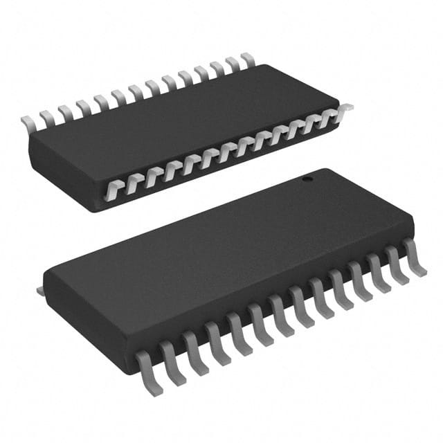
Allegro MicroSystems A3940KLWTR-T
- Part No.:
- A3940KLWTR-T
- Manufacturer:
- Allegro MicroSystems
- Category:
- Motor Drivers, Controllers
- Package:
- 28-SOIC (0.295", 7.50mm Width)
- Datasheet:
-
 A3940KLWTR-T.pdf
- Description:
- IC MOTOR DRIVER 7V-40V 28SOIC
- Quantity:
- Payment:

- Shipping:

Inventory:4,234
Please send an inquiry. Send us your inquiry, and we will respond immediately.
Product details
Overview
A3940KLWTR-T from Allegro MicroSystems is a full-bridge power MOSFET controller designed for automotive high-power motor drive applications. It delivers four high-current gate drive outputs, supports 100% duty cycle operation via integrated charge pump, and provides programmable dead-time adjustment (0.3–345 µs), VBB operating range of 7–40 V, and thermal shutdown at 172°C.
For engineers reviewing the A3940KLWTR-T datasheet, A3940KLWTR-T pinout, A3940KLWTR-T application, or A3940KLWTR-T equivalent, this page delivers verified technical context, validated pin functions, confirmed protection features (short-to-battery/ground, UV/OV, thermal), and real-world automotive motor control use cases - all grounded in the official Allegro A3940 datasheet Rev. 29319.100J.
Technical Context
The A3940KLWTR-T implements a dual-channel, n-channel MOSFET full-bridge driver with independent high-side (GHA/GHB) and low-side (GLA/GLB) gate outputs, each capable of sourcing up to 700 mA (25°C) and sinking up to 800 mA (25°C). Its internal charge pump (VCP = VBB + 9.5–11.8 V) enables DC operation without external bootstrap diodes.
It integrates two regulated supplies: VREG13 (12.6–14.0 V, 15 mA max) for gate drive and VREG5 (4.5–5.5 V, 4 mA load) for logic, plus fault detection circuitry with user-configurable thresholds via OVSET and VDSTH pins. Fault responses include latched short-circuit reporting and non-latched UV/OV/thermal shutdowns.
Key Specifications
| Parameter | Value and Actual Design Meaning |
|---|---|
| VBB Range | 7 V to 40 V - supports wide automotive battery voltage swings including cold-crank and load-dump conditions. |
| Gate Drive Output | GHA/GHB: VDSL(H) = VREG13 − 2.2 V (min), rSDU(on) = 4.0 Ω (25°C) - ensures robust turn-on of high-side n-MOSFETs. |
| Charge Pump Output | VCP = VBB + 9.5–11.8 V @ ICP = 15 mA - sustains high-side gate voltage for 100% duty cycle without external boost. |
| Dead Time Range | 0.3–345 µs - adjustable via RDEAD (12.1 kΩ–499 kΩ) and LONG pin to prevent shoot-through across wide FET switching speeds. |
| Fault Detection | VSTG(th) and VSTB(th) set by VDSTH (0.3–3.0 V); VBB(ov) user-adjustable from 16–39 V via OVSET - enables precise motor lead fault discrimination. |
| Thermal Protection | Thermal shutdown at TJ = 172°C with 12°C hysteresis - prevents irreversible damage during sustained overload or poor heatsinking. |
| Operating Temp | TJ = −40°C to +150°C - qualified for under-hood automotive environments per AEC-Q100 stress requirements. |
Pinout & Package
A3940KLWTR-T is supplied in a 28-pin wide-body SOIC package (KLW) with gull-wing leads and no exposed thermal pad. The package meets RoHS-compliant Pb-free requirements with 100% matte-tin leadframe plating.
| Pin/Terminal | Circuit Role | Design Meaning |
|---|---|---|
| 1 VDRAIN | Kelvin drain monitor | Provides accurate high-side drain-to-source voltage sensing for short-to-ground fault detection, isolated from power bus IR drop. |
| 2 LSS | Low-side source return | Reference node for low-side MOSFET source terminals and short-to-battery fault monitoring. |
| 3 GLB | Low-side gate drive B | Sinks up to 800 mA to turn on external n-MOSFET in phase B leg; supports synchronous rectification when SR = 1. |
| 4 SB | Motor phase B connection | Direct interface to motor winding B; negative terminal for CB bootstrap capacitor and reference for high-side driver floating supply. |
| 5 GHB | High-side gate drive B | Sources up to 700 mA to drive external n-MOSFET gate in phase B high-side; requires external series resistor for slew control. |
| 6 CB | Bootstrap capacitor B | Charged to VREG13 − 1.5 V when SB is low; lifts GHB gate above VBATT during high-side conduction. |
| 7 VIN | VREG13 input | Accepts VCP (charge pump output) or direct VBB ≥11 V to power 13 V gate drive regulator. |
| 8 VREG13 | 13 V gate drive supply | Stable 13.3 V output (±0.7 V) powering low-side drivers and charging bootstrap caps; shuts down during VBB undervoltage. |
| 9 CA | Bootstrap capacitor A | Same function as CB but for phase A; connects between GHA and SA terminals. |
| 10 GHA | High-side gate drive A | Phase A high-side driver output; identical electrical specs to GHB. |
| 11 SA | Motor phase A connection | Direct interface to motor winding A; negative terminal for CA bootstrap capacitor. |
| 12 GLA | Low-side gate drive A | Phase A low-side driver output; identical electrical specs to GLB. |
| 13 VBB | Battery supply input | Main power input (7–40 V); powers VREG5, enables charge pump, and triggers UV/OV faults. |
| 14 CP2 | Charge pump positive | Connects to positive side of external charge pump capacitor; required only if using internal charge pump. |
| 15 VCP | Charge pump output | Regulated boost voltage (VBB + 9.5–11.8 V) used as VIN for VREG13; connect to VBB if charge pump disabled. |
| 16 CP1 | Charge pump negative | Connects to negative side of external charge pump capacitor; leave open if charge pump unused. |
| 17 GND | Common ground | Analog/digital ground reference; electrically isolated from thermal pad in KLW package (unlike KLP). |
| 18 FAULT | Open-drain fault indicator | Asserts logic high (open-drain) on any fault condition; requires external pull-up to VREG5 or controller; causes automatic coast. |
| 19 OVSET | VBB overvoltage threshold | Analog input (0–0.9 V) setting VBB(ov) trip point from 16–39 V; driven by resistor divider from VREG5. |
| 20 VREG5 | 5 V logic supply | Stable 5.0 V output powering internal logic, OVSET/VDSTH networks, and FAULT pull-up; remains active during VBB UV. |
| 21 MODE | Current decay mode select | Logic 0 = fast-decay (both FETs off), Logic 1 = slow-decay (high-side off only); internal 50 kΩ pull-down. |
| 22 SR | Synchronous rectification enable | Logic 1 enables low-side FET conduction during off-time to reduce power loss; internal 50 kΩ pull-down. |
| 23 ENABLE | Driver enable control | Logic 1 enables PHASE/PWM control; logic 0 disables all gate outputs (coast); internal 50 kΩ pull-down. |
| 24 PHASE | Motor direction control | Logic 1 = forward (GHA/GLB active), Logic 0 = reverse (GHB/GLA active); internal 50 kΩ pull-down. |
| 25 RESET | Reset/sleep control | Logic 0 forces sleep mode (all regulators off, GHx/GLx = Z), clears latched faults; logic 1 enables normal operation. |
| 26 LONG | Dead time scaling | Logic 0 = short dead time (0.3–11 µs), Logic 1 = long dead time (8.3–345 µs); internal 50 kΩ pull-down. |
| 27 IDEAD | Dead time current set | Analog input (2 V reference) accepting 4–167 µA from RDEAD (12.1–499 kΩ) to program tdead. |
| 28 VDSTH | Drain-source threshold | Analog input (0.3–3.0 V) setting short-to-ground/battery fault thresholds; driven by resistor divider from VREG5. |
Key Features
| Feature | Design Value |
|---|---|
| Charge pump + bootstrap gate drive | Enables true 100% duty cycle operation of n-channel high-side MOSFETs without external diode or complex timing. |
| Programmable dead-time control | Two-stage adjustment (LONG + RDEAD) covers 0.3–345 µs to match diverse MOSFET switching speeds and prevent shoot-through. |
| Motor lead fault diagnostics | Dedicated VDRAIN and LSS sensing paths with user-set VDSTH threshold enable reliable short-to-battery and short-to-ground detection. |
| Dual regulated supplies | VREG13 (13.3 V/15 mA) powers gate drivers; VREG5 (5.0 V/4 mA) powers logic - both internally current-limited and fault-monitored. |
| Automotive-grade thermal protection | Thermal shutdown at 172°C with 12°C hysteresis ensures safe operation in under-hood environments without external sensors. |
Applications
| Electric Power Steering (EPS) | Automotive HVAC Blower |
|---|---|
|
Use Scenario: High-reliability bidirectional motor control in safety-critical steering assist systems requiring continuous torque delivery and fault resilience. IC Role / Device Role / Timing Role: Full-bridge gate driver controlling dual n-MOSFET H-bridge; manages PWM, direction, decay mode, and real-time fault response. Use Value: Integrated VBB UV/OV, thermal shutdown, and motor lead short detection eliminate need for external monitoring ICs, reducing BOM count and PCB area. |
Use Scenario: Variable-speed blower motor control in passenger cabin HVAC systems demanding quiet operation and energy efficiency. IC Role / Device Role / Timing Role: Gate driver enabling synchronous rectification (SR = 1) and programmable dead time to minimize conduction losses and EMI. Use Value: VREG5-powered OVSET/VDSTH networks allow precise, temperature-stable fault thresholds - critical for consistent performance across −40°C to +85°C ambient. |
| Engine Cooling Fan | Seat Motor Actuation |
|
Use Scenario: High-power radiator fan control subject to load dump transients (up to 40 V) and thermal cycling in engine bay. IC Role / Device Role / Timing Role: Robust gate driver with 40 V absolute max VBB rating and charge pump supporting 100% duty cycle for stall-torque hold. Use Value: Internal VREG13 regulator eliminates need for external 13 V supply, simplifying power architecture while maintaining gate drive integrity during battery dips. |
Use Scenario: Compact, low-noise seat position adjustment using small brushed DC motors with frequent direction reversals. IC Role / Device Role / Timing Role: Directional full-bridge controller using PHASE input and MODE-selectable decay modes to optimize torque ripple and acoustic noise. Use Value: Programmable dead time (via RDEAD) allows fine-tuning for low-inductance seat motor windings, preventing cross-conduction during rapid direction changes. |
Equivalent & Alternatives
The following parts are listed as comparable options for similar full-bridge gate driver applications.
| Alternative Part | Technical Difference | Application Difference | Selection Advice |
|---|---|---|---|
| A3941KLPTR-T | Pin-compatible successor with enhanced thermal performance (TJ max = 175°C), improved VCP regulation accuracy (±2%), and updated fault latch behavior. | Designed for new designs requiring extended lifetime reliability and tighter gate drive stability under high-temperature operation. | Select A3941KLPTR-T for new designs; A3940KLWTR-T remains viable for legacy repair or continuity builds where KLW SOIC footprint is mandatory. |
| MP6532DS-LF-Z | Monolithic 2-phase BLDC gate driver (not full-bridge discrete control); lacks VDRAIN Kelvin sense, OVSET/VDSTH analog programming, and VREG13/VREG5 dual regulators. | Targeted at sensorless BLDC commutation in fans/pumps; not suitable for brushed DC motor control with diagnostic requirements. | Only consider MP6532DS-LF-Z if migrating to BLDC topology and accepting reduced fault granularity and no analog threshold tuning. |
Compared with A3941KLPTR-T, A3940KLWTR-T offers identical pinout and functional coverage but lower thermal shutdown threshold and looser VCP regulation - making it suitable for cost-sensitive legacy automotive repairs. MP6532DS-LF-Z diverges fundamentally in architecture and diagnostic capability, limiting cross-application use.
Availability
A3940KLWTR-T is available at Aetrix Electronics and suitable for automotive EPS modules, HVAC blowers, engine cooling fans, and seat actuation systems requiring stable component supply despite end-of-life status.
Supply support for A3940KLWTR-T includes scheduled delivery planning, volume procurement assistance, BOM continuity management, traceable sourcing, and lifecycle availability coordination for OEM customers, industrial embedded developers, connected-device designers, and electronics production programs.
Manufacturer
Allegro MicroSystems is a global leader in precision sensing and power ICs, specializing in magnetic sensors, motor drivers, and power management solutions for automotive and industrial markets.
The A3940 product line was engineered specifically for high-reliability, high-power brushed DC motor control in automotive under-hood applications - emphasizing integrated protection, wide input voltage tolerance, and diagnostic transparency.
FAQ
What is the recommended replacement for A3940KLWTR-T in new designs?
The A3941KLPTR-T is the officially recommended substitution per Allegro documentation. While A3940KLWTR-T is discontinued, A3941KLPTR-T maintains pin compatibility and adds tighter VCP regulation (±2%), higher thermal shutdown threshold (175°C), and refined fault latch behavior - making it the preferred choice for new automotive motor control designs requiring full-bridge gate drive functionality.
Does A3940KLWTR-T support 100% duty cycle operation for high-side n-MOSFETs?
Yes, A3940KLWTR-T supports true 100% duty cycle operation via its integrated charge pump (VCP output) combined with bootstrap gate drive. The charge pump generates VCP = VBB + 9.5–11.8 V, ensuring sufficient gate-to-source voltage for high-side n-MOSFETs even when the bridge output is held continuously high - eliminating reliance on external diodes or complex timing constraints.
How does A3940KLWTR-T detect short-to-ground and short-to-battery faults?
A3940KLWTR-T uses dedicated sensing paths: VDRAIN (Kelvin-connected to high-side drains) monitors short-to-ground during high-side conduction, while LSS serves as reference for short-to-battery detection during low-side conduction. Thresholds are set via the VDSTH pin (0.3–3.0 V), and fault evaluation is delayed by one or two dead times post-switching to avoid false triggers from transient voltage spikes.
What are the key differences between the A3940KLWTR-T and A3940KLPTR-T packages?
A3940KLWTR-T uses a 28-pin wide-body SOIC (KLW) package without an exposed thermal pad, whereas A3940KLPTR-T uses a 28-pin TSSOP with exposed thermal pad (KLP). Both are Pb-free with matte-tin plating, but the KLP package offers superior thermal dissipation for high-power continuous operation, while KLW provides higher creepage/clearance and compatibility with legacy SOIC footprints.
Can A3940KLWTR-T operate with a 5 V logic supply?
No, A3940KLWTR-T does not accept 5 V as its primary supply. Its VBB input requires 7–40 V to power internal regulators (VREG5 and VREG13) and gate drivers. However, it provides a regulated 5 V output (VREG5) for external logic circuits - this output is derived from VBB and cannot be used as an input source for the device itself.
A3940KLWTR-T Specifications
- Product attributes
- Attribute value
- Manufacturer:
- Allegro MicroSystems
- Series:
- -
- Package/Case:
- 28-SOIC (0.295", 7.50mm Width)
- Packaging:
- Tape & Reel (TR)
- Product Status:
- Obsolete
- Motor Type - Stepper:
- -
- Motor Type - AC, DC:
- Brushed DC
- Function:
- Controller - Commutation, Direction Management
- Output Configuration:
- Pre-Driver - Half Bridge (2)
- Interface:
- Parallel
- Technology:
- Power MOSFET
- Step Resolution:
- -
- Applications:
- -
- Current - Output:
- -
- Voltage - Supply:
- 7V ~ 40V
- Voltage - Load:
- -
- Operating Temperature:
- -40°C ~ 135°C (TA)
- Grade:
- Automotive
- Qualification:
- -
- Mounting Type:
- Surface Mount
- Supplier Device Package:
- 28-SOIC
A3940KLWTR-T FAQ
1.How can I place an order for A3940KLWTR-T through Aetrix?
Please submit a Request for Quotation (RFQ) for A3940KLWTR-T on Aetrix. Our sales agent will provide a competitive quotation and guide you through the order confirmation once you accept the terms.
2.Are the price and stock information for A3940KLWTR-T reliable?
The price and inventory of A3940KLWTR-T are updated periodically and may fluctuate due to market conditions. Stock and pricing data are typically refreshed every 24 hours. Quotation validity for A3940KLWTR-T is usually 5 days.
3.What payment methods are accepted for A3940KLWTR-T?
We accept Wire Transfer, PayPal, Credit Card, Western Union, MoneyGram, and Escrow for A3940KLWTR-T transactions.
Note: Certain payment methods may incur a processing fee.
4.How is shipping managed for A3940KLWTR-T?
A3940KLWTR-T orders can be shipped via leading logistics carriers, including DHL, UPS, FedEx, TNT, or Registered Mail.
Once your A3940KLWTR-T order is processed, you will receive an email with the shipment details and tracking number.
Note: Tracking information may take up to 24 hours to appear. Express delivery typically takes 3–5 business days.
5.How can I obtain technical support or documentation for A3940KLWTR-T?
For technical support, including A3940KLWTR-T datasheets, pinout diagrams, or application guidance, please contact our engineering support team. They can provide detailed documentation and assistance for your A3940KLWTR-T requirements.
6.How does Aetrix verify that A3940KLWTR-T is sourced from the original manufacturer or authorized distributors?
All A3940KLWTR-T products on Aetrix are procured from qualified distributors and authorized channels. Our dedicated quality assurance team conducts strict verification, including traceability checks and, if necessary, third-party testing. This ensures that A3940KLWTR-T meets industry standards.
7.What is the process for return or replacement of A3940KLWTR-T?
All A3940KLWTR-T units undergo pre-shipment inspection (PSI). If there is an issue with A3940KLWTR-T, returns or replacements are accepted under the following conditions:
1.Quantity discrepancies, incorrect items, or visible external defects (such as breakage or corrosion), acknowledged by Aetrix.
2.The issue is reported within 90 days of delivery.
3.The A3940KLWTR-T part is unused and in its original packaging.
Return procedure for A3940KLWTR-T:
1.Submit a request within 90 days.
2.Obtain a Return Material Authorization (RMA) from Aetrix.
A3940KLWTR-T Tags

-
DRV2603RUNR
Texas Instruments

-
DRV8837CDSGR
Texas Instruments

-
DRV8837DSGR
Texas Instruments
-
DRV8838DSGR
Texas Instruments

-
DRV8839DSSR
Texas Instruments

-
EMC2301-1-ACZL-TR
Microchip Technology
-
DRV8231ADSGR
Texas Instruments

-
EMC2302-2-AIZL-TR
Microchip Technology

-
DRV8800PWPR
Texas Instruments
-
DRV8835DSSR
Texas Instruments

-
EMC2303-1-KP-TR
Microchip Technology

-
DRV8876PWPR
Texas Instruments
Tech Hub

A practical engineering and sourcing framework covering lifecycle verification, lifetime-buy calculations, replacement qualification, supplier checks and counterfeit-risk controls.

TTL and CMOS logic families differ in thresholds, loading, output drive, power and timing. This engineering guide compares 74HC and 74HCT, calculates noise margins and checks 3.3 V/5 V compatibility.

A practical engineering guide to 3.3V and 5V logic compatibility, input thresholds, resistor dividers, translator ICs, MOSFET level shifting, I2C pull-ups, timing limits and power-sequencing risks.

The 74HC595 uses push-pull logic outputs, while the TPIC6B595 uses 50 V open-drain DMOS sinks for higher-power loads. This guide compares timing, current limits, 3.3 V interfacing, load wiring, thermal…

The 74HC595 converts serial data into eight stable parallel outputs. This guide covers pin functions, shift and storage timing, OE and MR behavior, drive-current limits, cascading, voltage compatibilit…

A technical comparison of level-sensitive latches and edge-triggered flip-flops, covering timing windows, setup and hold limits, master–slave operation, time borrowing, race-through, HDL inference and…

A D latch stores one bit while Enable controls when data can pass. This reference covers gate-level operation, truth tables, transparency, setup and hold timing, LE versus OE, common ICs and practical …

An SR latch stores one bit through cross-coupled feedback. This engineering reference covers NOR and NAND implementations, truth tables, forbidden-state recovery, gated operation, switch debouncing, fa…

Latch circuits retain one bit through feedback. This technical reference covers SR and D latches, truth tables, transparency, timing limits, latch-versus-flip-flop behavior, applications and common log…

An engineering guide to LED driver operation, constant-current and constant-voltage outputs, linear and switching topologies, dimming, IC selection, calculations, replacement compatibility, and fault c…


