
 My Inquiry
 My Account


Allegro MicroSystems A3959SLP
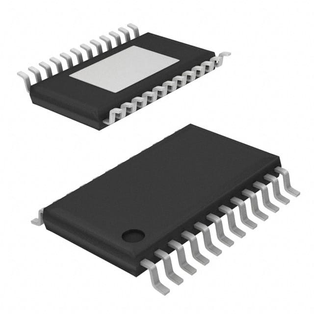
- Part No.:
- A3959SLP
- Manufacturer:
- Allegro MicroSystems
- Category:
- Motor Drivers, Controllers
- Package:
- 28-TSSOP (0.173", 4.40mm Width) Exposed Pad
- Datasheet:
-
 A3959SLP.pdf
- Description:
- IC MOTOR DRVR 4.5V-5.5V 28TSSOP
- Quantity:
- Payment:

- Shipping:

Inventory:3,063
Please send an inquiry. Send us your inquiry, and we will respond immediately.
Product details
Overview
A3959SLP from Allegro MicroSystems is a DMOS full-bridge PWM motor driver IC designed for bidirectional DC motor control with ±3 A output current and 50 V load supply capability. It implements internal fixed off-time current regulation, synchronous rectification, and selectable slow/fast/mixed decay modes via PFD1/PFD2 inputs. Used in industrial actuators, robotic joints, and precision positioning systems where thermal efficiency and current accuracy are critical.
For engineers reviewing the A3959SLP datasheet, A3959SLP pinout, A3959SLP application, or A3959SLP equivalent, this page delivers verified package mapping (28-pin TSSOP-LP), confirmed thermal pad grounding, validated current-sense architecture (VREF/10RS), and real-world decay-mode timing behavior - all essential for motor driver layout, thermal design, and PWM loop stability analysis.
Technical Context
The A3959SLP integrates dual DMOS H-bridge drivers with independent source/sink gate drive, an internal 4.25 MHz oscillator (set by ROSC resistor), and a fixed 24 µs off-time PWM timer. Its current regulation relies on analog sensing at the SENSE pin with trip threshold defined as ITRIP = VREF/10RS, enabling precise ±3 A peak current control without external op-amps.
Thermal management is implemented via junction-to-pad thermal resistance of 2°C/W (RθJP) and integrated thermal shutdown at 165°C with 15°C hysteresis. Synchronous rectification activates during decay cycles to replace body-diode conduction, reducing power loss by minimizing voltage drop across low rDS(on) (270 mΩ typical) outputs.
Key Specifications
| Parameter | Value and Actual Design Meaning |
|---|---|
| Output Current | ±3 A continuous - supports medium-power DC motors up to ~150 W at 50 V with appropriate heatsinking |
| Load Supply Voltage | 9.5–50 V - compatible with 12 V, 24 V, and 48 V industrial bus systems |
| rDS(on) (Typ.) | 270 mΩ per channel - limits conduction loss to ≤2.43 W per switch at ±3 A |
| Fixed Off-Time | 24 µs (96 oscillator cycles @ 4.25 MHz) - sets minimum PWM frequency and decay duration baseline |
| Junction-to-Pad RθJP | 2°C/W - enables high-power dissipation when mounted on 4-layer PCB with thermal vias to exposed pad |
| Thermal Shutdown | 165°C activation with 15°C hysteresis - prevents latch-up during overload while allowing recovery without power cycle |
| VREF Input Range | 0–VDD (5.0 V typical) - allows scalable current limit from 0.5 A to 3 A using standard resistor values |
Pinout & Package
Package: 28-pin TSSOP (suffix 'LP') with exposed thermal pad (pin 28); all ground pins (7, 8, 28) must be connected together at the pad for optimal thermal and electrical performance.
| Pin/Terminal | Circuit Role | Design Meaning |
|---|---|---|
| 1, 7, 8, 28 | GROUND | Common return for logic, charge pump, and power grounds; pin 28 is thermal pad - requires low-impedance solder connection |
| 2, 3 | CP1 / CP2 | Charge pump capacitor terminals - require 0.22 µF ceramic cap between them for high-side gate drive generation |
| 4 | PHASE | Direction control input - high/low selects OUTA/OUTB polarity for forward/reverse motor rotation |
| 5 | ROSC | Oscillator timing resistor - 51 kΩ to VDD sets 4.25 MHz internal clock for PWM timing consistency |
| 6 | CP | Charge pump reservoir - connects to 0.22 µF cap to VBB for stable high-side gate voltage |
| 9 | VDD | Logic supply input - must be 4.5–5.5 V; powers internal logic, regulators, and gate drivers |
| 10 | ENABLE | PWM enable input - high enables bridge; low disables source driver or both drivers depending on EXT MODE state |
| 12, 14 | PFD2 / PFD1 | Decay mode select - binary encoding (00=slow, 01/10=mixed, 11=fast) controls recirculation path during off-time |
| 13 | BLANK | Comparator blanking control - extends blank time to 12/fOSC to suppress sense spikes during turn-on |
| 15 | REF | Analog reference input - sets current limit via ITRIP = VREF/10RS; accepts 0–5 V range |
| 16 | EXT MODE | External PWM mode selector - high = slow decay, low = fast decay during ENABLE chopping |
| 18, 24 | OUTA / OUTB | H-bridge output terminals - connect directly to motor terminals; each rated for ±3 A continuous |
| 21 | SENSE | Current sense input - connects to low-side sense resistor (RS); referenced to device ground, not PCB ground plane |
| 23 | SLEEP | Low-power mode control - logic low disables regulator, charge pump, and drivers, reducing quiescent current to ≤20 µA |
| 26 | VREG | Internal regulator output - supplies sink-side gate drive; requires 0.22 µF decoupling cap to ground |
| 27 | LOAD SUPPLY (VBB) | High-current motor supply input - accepts 9.5–50 V; decoupled with ≥47 µF electrolytic capacitor |
Key Features
| Feature | Design Value |
|---|---|
| Synchronous Rectification | Replaces body-diode conduction with active low-rDS(on) FET paths during decay, cutting power loss by >40% vs. passive diodes |
| Mixed Decay Mode | Combines 15% or 48% fast decay followed by slow decay - reduces audible noise and torque ripple in mid-speed operation |
| Internal Oscillator + ROSC | Eliminates need for external clock source; 51 kΩ resistor yields stable 4.25 MHz timing for consistent 24 µs off-time |
| Crossover-Current Protection | Prevents shoot-through via 300–1000 ns delay between source/sink switching - ensures safe dead-time without external logic |
| Thermal Pad Integration | Exposed pad (pin 28) provides 2°C/W junction-to-board thermal path - enables 3.1 W continuous dissipation on 4-layer PCB |
Applications
| Industrial Actuators | Robotic Joint Drivers |
|---|---|
|
Use Scenario: Precision linear actuator in automated valve control requiring smooth bidirectional motion and stall-current protection. IC Role / Device Role / Timing Role: Full-bridge motor driver with internal current regulation and synchronous rectification to maintain torque linearity across 0–100% duty cycle. Use Value: Enables closed-loop current control without external amplifiers; mixed-decay mode suppresses mechanical resonance at 20–80 Hz operating band. |
Use Scenario: Compact elbow/wrist joint in collaborative robot arm needing compact 28-pin TSSOP footprint and low thermal resistance. IC Role / Device Role / Timing Role: Bidirectional H-bridge controller managing inertia-limited acceleration/deceleration with braking via slow-decay mode. Use Value: Exposed thermal pad (RθJP = 2°C/W) sustains 3 A continuous under 60°C ambient - eliminates need for external heatsink in space-constrained enclosures. |
| Medical Infusion Pumps | Automated Test Equipment (ATE) |
|
Use Scenario: Peristaltic pump in infusion system requiring microstepped flow control and fault-safe shutdown on overtemperature. IC Role / Device Role / Timing Role: Current-regulated motor driver with thermal shutdown hysteresis (15°C) and UVLO to prevent erratic behavior during brownout. Use Value: Internal 165°C thermal cutoff and 3.9–4.45 V UVLO window ensure fail-safe motor stop without software intervention - meets IEC 60601-1 creepage requirements. |
Use Scenario: Positioner stage in semiconductor probe station demanding repeatable 0.1% current accuracy and minimal EMI during rapid direction reversal. IC Role / Device Role / Timing Role: PWM-controlled H-bridge with blanking timer (6/fOSC or 12/fOSC) to reject sense-node transients during PHASE toggling. Use Value: BLANK input extends comparator disable window to eliminate false trips from reverse-recovery spikes - maintains current regulation integrity at 20 kHz PWM. |
Equivalent & Alternatives
The following parts are listed as comparable options for similar full-bridge PWM motor driver applications.
| Alternative Part | Technical Difference | Application Difference | Selection Advice |
|---|---|---|---|
| TB6612FNG | Lower 1.2 A continuous rating, no internal charge pump - requires external high-side gate drive or bootstrap circuitry | Better suited for low-power portable devices; lacks thermal pad and mixed-decay mode | Select when board space is constrained and motor current ≤1.2 A; avoid for 50 V bus or high-thermal-load designs |
| DRV8876N | Integrated current sense amplifier (not just comparator), 3.6 A rating, but higher rDS(on) (350 mΩ) and no synchronous rectification | Preferred for designs needing analog current feedback; less efficient at high PWM frequencies due to body-diode conduction | Choose when closed-loop current monitoring is required; accept 20–30% higher conduction loss vs. A3959SLP at 3 A |
Compared with TB6612FNG and DRV8876N, the A3959SLP uniquely combines ±3 A capability, synchronous rectification, mixed-decay control, and 2°C/W thermal resistance in a single 28-pin TSSOP - making it optimal for thermally demanding, medium-power industrial motion systems where efficiency and layout simplicity are prioritized over analog current telemetry.
Availability
A3959SLP is available at Aetrix Electronics and suitable for industrial actuators, robotic joint modules, medical infusion pumps, and automated test equipment requiring stable component supply, long-term lifecycle support, and traceable sourcing.
Supply support for A3959SLP includes scheduled delivery planning, volume procurement assistance, BOM continuity management, traceable sourcing, and lifecycle availability coordination for OEM customers, industrial embedded developers, connected-device designers, and electronics production programs.
Manufacturer
Allegro MicroSystems is a U.S.-based designer of high-performance magnetic sensors and power ICs, specializing in motion control, energy-efficient power conversion, and robust automotive-grade semiconductors.
The A3959SLP belongs to Allegro's DMOS full-bridge motor driver product line, engineered specifically for thermally constrained, high-reliability industrial motion systems requiring precise current regulation and integrated protection without external support components.
FAQ
What is the maximum continuous output current supported by the A3959SLP?
The A3959SLP supports ±3 A continuous output current under specified thermal conditions - including use of a 4-layer PCB with thermal vias to the exposed pad, ambient temperature ≤85°C, and proper decoupling. Peak current up to ±6 A is allowed for pulses <3 µs. Actual current capability depends on VBB, duty cycle, and heatsinking; the device will thermally shut down at 165°C junction temperature to protect itself. The A3959SLP datasheet specifies 3.1 W package power dissipation for the LP package under JEDEC 4-layer conditions.
How does the A3959SLP implement current regulation without an external op-amp?
The A3959SLP uses an internal analog current-sense comparator referenced to VREF, with trip threshold calculated as ITRIP = VREF/10RS. The device measures voltage across an external sense resistor (RS) connected to the SENSE pin and compares it to VREF/10. When the sensed voltage exceeds this threshold, the internal PWM timer initiates a fixed 24 µs off-time period. This fully integrated method eliminates the need for external amplification or compensation networks - a key differentiator of the A3959SLP versus discrete gate-driver solutions.
Can the A3959SLP be used for motor braking, and how is it configured?
Yes, the A3959SLP supports active motor braking by configuring EXT MODE = high (slow decay) and applying a chopped ENABLE signal. In this mode, both sink drivers conduct during the off-time, shorting the motor terminals and dissipating kinetic energy through the windings and MOSFETs. Note that braking current is not regulated by the internal current-sense circuit (since it bypasses RS), so peak brake current must be limited externally or by controlling ENABLE duty cycle. The A3959SLP's 50 V rating and thermal shutdown provide inherent protection during aggressive braking events.
What is the role of the exposed thermal pad (pin 28) on the A3959SLP package?
The exposed thermal pad (pin 28) on the A3959SLP serves as the primary thermal conduction path from the silicon die to the PCB, with a specified junction-to-pad thermal resistance (RθJP) of 2°C/W. It must be soldered directly to a large copper area with multiple thermal vias to internal ground planes. Unlike standard ground pins, pin 28 is electrically tied to ground but functions primarily for heat extraction - enabling the A3959SLP to sustain 3.1 W of power dissipation on a 4-layer board. Failure to properly connect this pad results in excessive junction temperature and premature thermal shutdown.
Does the A3959SLP require special power-up sequencing?
No, the A3959SLP does not require special power-up sequencing. Its internal UVLO circuit monitors VDD and disables outputs until VDD rises above 4.2 V (typical), while charge pump and VREG circuits are self-managed. The device safely powers up with VBB applied before or after VDD, and no external reset or delay circuitry is needed. This simplifies system design and improves reliability in applications with unregulated or staggered supply rails - a documented feature of the A3959SLP in Allegro's official documentation.
A3959SLP Specifications
- Product attributes
- Attribute value
- Manufacturer:
- Allegro MicroSystems
- Series:
- -
- Package/Case:
- 28-TSSOP (0.173", 4.40mm Width) Exposed Pad
- Packaging:
- Tube
- Product Status:
- Obsolete
- Motor Type - Stepper:
- -
- Motor Type - AC, DC:
- Brushed DC
- Function:
- Driver - Fully Integrated, Control and Power Stage
- Output Configuration:
- Half Bridge (2)
- Interface:
- Parallel
- Technology:
- DMOS
- Step Resolution:
- -
- Applications:
- General Purpose
- Current - Output:
- 3A
- Voltage - Supply:
- 4.5V ~ 5.5V
- Voltage - Load:
- 9.5V ~ 50V
- Operating Temperature:
- -20°C ~ 150°C (TJ)
- Grade:
- -
- Qualification:
- -
- Mounting Type:
- Surface Mount
- Supplier Device Package:
- 28-TSSOP-EP
A3959SLP FAQ
1.How can I place an order for A3959SLP through Aetrix?
Please submit a Request for Quotation (RFQ) for A3959SLP on Aetrix. Our sales agent will provide a competitive quotation and guide you through the order confirmation once you accept the terms.
2.Are the price and stock information for A3959SLP reliable?
The price and inventory of A3959SLP are updated periodically and may fluctuate due to market conditions. Stock and pricing data are typically refreshed every 24 hours. Quotation validity for A3959SLP is usually 5 days.
3.What payment methods are accepted for A3959SLP?
We accept Wire Transfer, PayPal, Credit Card, Western Union, MoneyGram, and Escrow for A3959SLP transactions.
Note: Certain payment methods may incur a processing fee.
4.How is shipping managed for A3959SLP?
A3959SLP orders can be shipped via leading logistics carriers, including DHL, UPS, FedEx, TNT, or Registered Mail.
Once your A3959SLP order is processed, you will receive an email with the shipment details and tracking number.
Note: Tracking information may take up to 24 hours to appear. Express delivery typically takes 3–5 business days.
5.How can I obtain technical support or documentation for A3959SLP?
For technical support, including A3959SLP datasheets, pinout diagrams, or application guidance, please contact our engineering support team. They can provide detailed documentation and assistance for your A3959SLP requirements.
6.How does Aetrix verify that A3959SLP is sourced from the original manufacturer or authorized distributors?
All A3959SLP products on Aetrix are procured from qualified distributors and authorized channels. Our dedicated quality assurance team conducts strict verification, including traceability checks and, if necessary, third-party testing. This ensures that A3959SLP meets industry standards.
7.What is the process for return or replacement of A3959SLP?
All A3959SLP units undergo pre-shipment inspection (PSI). If there is an issue with A3959SLP, returns or replacements are accepted under the following conditions:
1.Quantity discrepancies, incorrect items, or visible external defects (such as breakage or corrosion), acknowledged by Aetrix.
2.The issue is reported within 90 days of delivery.
3.The A3959SLP part is unused and in its original packaging.
Return procedure for A3959SLP:
1.Submit a request within 90 days.
2.Obtain a Return Material Authorization (RMA) from Aetrix.
A3959SLP Tags

-
DRV2603RUNR
Texas Instruments

-
DRV8837CDSGR
Texas Instruments

-
DRV8837DSGR
Texas Instruments
-
DRV8838DSGR
Texas Instruments

-
DRV8839DSSR
Texas Instruments

-
EMC2301-1-ACZL-TR
Microchip Technology
-
DRV8231ADSGR
Texas Instruments

-
EMC2302-2-AIZL-TR
Microchip Technology

-
DRV8800PWPR
Texas Instruments
-
DRV8835DSSR
Texas Instruments

-
EMC2303-1-KP-TR
Microchip Technology

-
DRV8876PWPR
Texas Instruments
Tech Hub

A practical engineering and sourcing framework covering lifecycle verification, lifetime-buy calculations, replacement qualification, supplier checks and counterfeit-risk controls.

TTL and CMOS logic families differ in thresholds, loading, output drive, power and timing. This engineering guide compares 74HC and 74HCT, calculates noise margins and checks 3.3 V/5 V compatibility.

A practical engineering guide to 3.3V and 5V logic compatibility, input thresholds, resistor dividers, translator ICs, MOSFET level shifting, I2C pull-ups, timing limits and power-sequencing risks.

The 74HC595 uses push-pull logic outputs, while the TPIC6B595 uses 50 V open-drain DMOS sinks for higher-power loads. This guide compares timing, current limits, 3.3 V interfacing, load wiring, thermal…

The 74HC595 converts serial data into eight stable parallel outputs. This guide covers pin functions, shift and storage timing, OE and MR behavior, drive-current limits, cascading, voltage compatibilit…

A technical comparison of level-sensitive latches and edge-triggered flip-flops, covering timing windows, setup and hold limits, master–slave operation, time borrowing, race-through, HDL inference and…

A D latch stores one bit while Enable controls when data can pass. This reference covers gate-level operation, truth tables, transparency, setup and hold timing, LE versus OE, common ICs and practical …

An SR latch stores one bit through cross-coupled feedback. This engineering reference covers NOR and NAND implementations, truth tables, forbidden-state recovery, gated operation, switch debouncing, fa…

Latch circuits retain one bit through feedback. This technical reference covers SR and D latches, truth tables, transparency, timing limits, latch-versus-flip-flop behavior, applications and common log…

An engineering guide to LED driver operation, constant-current and constant-voltage outputs, linear and switching topologies, dimming, IC selection, calculations, replacement compatibility, and fault c…


