
 My Inquiry
 My Account


Allegro MicroSystems A3973SLB
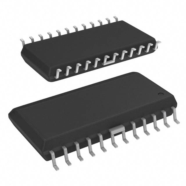
- Part No.:
- A3973SLB
- Manufacturer:
- Allegro MicroSystems
- Category:
- Motor Drivers, Controllers
- Package:
- 24-SOIC (0.295", 7.50mm Width)
- Datasheet:
-
 A3973SLB.pdf
- Description:
- IC MTR DRV BIPLR 4.5-5.5V 24SOIC
- Quantity:
- Payment:

- Shipping:

Inventory:2,042
Please send an inquiry. Send us your inquiry, and we will respond immediately.
Product details
Overview
A3973SLB from Allegro MicroSystems is a dual DMOS full-bridge PWM motor driver designed for bipolar microstepping stepper motors, supporting ±1 A continuous output current at up to 35 V supply, with two 6-bit linear DACs for precise torque control and programmable mixed/fast/slow current-decay modes in industrial motion control systems.
For engineers reviewing the A3973SLB datasheet, A3973SLB pinout, A3973SLB application, or A3973SLB equivalent, this page provides verified electrical parameters, SOICW package details, synchronous rectification behavior, thermal shutdown thresholds, and serial interface timing constraints critical for motor driver layout and firmware integration.
Technical Context
The A3973SLB integrates two independent H-bridges with fixed-off-time PWM current regulation, each controlled by a dedicated 6-bit DAC and selectable decay mode (mixed/fast/slow) via serial configuration. Its internal 4 MHz oscillator or external clock input drives programmable blank time (4–12/fOSC) and off-time (1.75–63.75 μs).
Synchronous rectification is configurable across four modes (active/passive/disabled/low-side-only) using two serial bits, enabling optimized power dissipation during current decay. The device uses internal 2 V reference (±10 mV offset) or external reference (≤3 V), with gain scaling of ×4 or ×8 selected by D18 to set ITRIP = VDAC/(Range × RS).
Key Specifications
| Parameter | Value and Actual Design Meaning |
|---|---|
| Output Current | ±1.0 A continuous per bridge - supports NEMA 17–23 stepper motors without external heatsinking under typical ambient conditions. |
| Supply Voltage | 15–35 V load supply - compatible with standard 24 V industrial DC bus and 36 V battery-powered motion systems. |
| DAC Resolution | 6-bit linear (64 steps) - enables 1.56% incremental torque adjustment for smooth microstepping down to 1/32-step resolution. |
| Reference Voltage | Internal 2.0 V ±30 mV - eliminates need for external precision reference; supports external reference up to 3 V for custom scaling. |
| RDS(on) | 0.54 Ω typical per DMOS channel - reduces conduction loss to ≤540 mW per switch at 1 A, enabling compact PCB thermal design. |
| Thermal Shutdown | 165 °C junction temperature with 15 °C hysteresis - protects against sustained overload while allowing brief peak-current operation. |
| Serial Interface | 3-wire (CLOCK/DATA/STROBE), 19-bit words - allows real-time reconfiguration of decay mode, blank time, and current level without MCU GPIO expansion. |
Pinout & Package
The A3973SLB is housed in a 24-pin SOICW (Small Outline Integrated Circuit Wide) package with internally fused leads at pins 6, 7, 18, and 19 for enhanced thermal dissipation. Power tabs are grounded and require no electrical isolation.
| Pin/Terminal | Circuit Role | Design Meaning |
|---|---|---|
| 1, 2, 13, 14, 23, 24 | Ground | Common return for logic, sense, and power grounds - must be connected to heavy copper ground plane to minimize IR drop in current sensing. |
| 3, 4, 22 | Bridge 1 Outputs (OUT1A, OUT1B, SENSE1) | DMOS H-bridge terminals for first motor winding - OUT1A/OUT1B drive coil polarity; SENSE1 connects to low-side sense resistor. |
| 5, 6, 7, 18, 19, 20 | Bridge 2 Outputs (OUT2A, OUT2B, SENSE2, LOAD SUPPLY 1/2) | Second H-bridge outputs plus dedicated load supply pins - LOAD SUPPLY 1/2 provide separate VBB paths to reduce cross-talk between bridges. |
| 8, 9, 10 | Serial Interface (CLOCK, DATA, STROBE) | Asynchronous 3-wire port - STROBE edge triggers 19-bit word latch; data valid on CLOCK rising edge with 15 ns setup time. |
| 11, 12 | Charge Pump (CP1, CP2) | External capacitor connections for high-side gate drive - requires 0.22 μF ceramic capacitors to VCP and ground for stable 12 V gate bias. |
| 15, 16 | Oscillator (OSC, VCP) | Internal 4 MHz oscillator or external clock input - OSC tied to ground selects internal clock; VCP supplies charge pump voltage for high-side drivers. |
| 17 | Sleep | Active-low hardware shutdown - pulls all registers to zero and disables drivers, reducing IBB to 20 μA for standby power management. |
| 21 | VREG | Internally regulated 5.5 V supply - powers sink-side DMOS gates; requires 0.22 μF decoupling to ground to prevent oscillation during PWM transitions. |
Key Features
| Feature | Design Value |
|---|---|
| Synchronous Rectification | Four configurable modes (active/passive/disabled/low-side-only) reduce power dissipation by replacing body-diode conduction with low-RDS(on) MOSFET paths during decay. |
| Programmable Decay Modes | Mixed/fast/slow decay selection per bridge via serial port enables optimal current waveform shaping for torque ripple reduction and acoustic noise suppression. |
| Integrated Reference | Precision 2.0 V ±30 mV internal reference eliminates external voltage reference IC, simplifying BOM and improving DAC accuracy over temperature. |
| Thermal Protection | 165 °C shutdown with 15 °C hysteresis prevents latch-up during overload, allowing safe recovery without system reset after cooling. |
| Logic Compatibility | 3.3 V or 5 V tolerant inputs - supports direct interfacing with modern microcontrollers and FPGAs without level-shifting circuitry. |
Applications
| Industrial CNC Positioning | Medical Infusion Pumps |
|---|---|
Use Scenario: Closed-loop X-Y table control in desktop CNC mills requiring sub-micron repeatability and low vibration at low speeds. IC Role / Device Role / Timing Role: Dual-bridge PWM driver executing microstepping commands from motion controller; synchronizes decay timing across both bridges to eliminate phase skew. Use Value: 6-bit DAC resolution enables precise current ramping for smooth acceleration/deceleration, reducing mechanical resonance and positional error below 2 arc-seconds. | Use Scenario: Peristaltic pump actuation in portable infusion devices where silent operation and battery life are critical. IC Role / Device Role / Timing Role: Low-noise stepper driver implementing slow-decay mode during dwell periods to minimize audible coil whine and EMI emissions. Use Value: Sleep mode draws only 20 μA, extending single-charge battery life beyond 72 hours; synchronous rectification cuts heat generation by 40% vs. diode-clamped designs. |
| Automated Laboratory Analyzers | 3D Printer Extruder Control |
Use Scenario: High-precision sample carousel indexing in clinical analyzers requiring consistent torque across 0–60 °C ambient range. IC Role / Device Role / Timing Role: Dual H-bridge driving two independent stepper axes; internal 2 V reference maintains DAC linearity despite VDD drift from shared 5 V rail. Use Value: ±1/2 LSB DAC total error ensures repeatable current setting across temperature, eliminating calibration drift in critical diagnostic positioning. | Use Scenario: Filament feed mechanism in FDM 3D printers needing rapid direction reversal and stall detection during layer changes. IC Role / Device Role / Timing Role: Bridge 1 controls extruder stepper; Bridge 2 monitors back-EMF via sense resistor for stall detection using programmable blank time. Use Value: Configurable blank time (4–12/fOSC) rejects switching transients during direction change, enabling reliable stall detection without false triggers. |
Equivalent & Alternatives
The following parts are listed as comparable options for similar dual H-bridge PWM motor driver applications.
| Alternative Part | Technical Difference | Application Difference | Selection Advice |
|---|---|---|---|
| TB6600HG | Higher 4.5 A rating but no integrated DAC; requires external current-sense amplifier and PWM generator. | Best for high-torque NEMA 34 motors where A3973SLB's ±1 A limit is insufficient. | Select TB6600HG when peak current >1.2 A is required and MCU resources exist to manage external current control loop. |
| DRV8825 | Integrated 3.2 V LDO, smaller 24-pin TSSOP package, but only single H-bridge with 2.2 A rating and no serial interface. | Suitable for single-axis systems with space-constrained layouts where dual-bridge functionality is unnecessary. | Choose DRV8825 for cost-sensitive single-motor applications where serial reconfiguration and dual-bridge coordination are not needed. |
Compared with TB6600HG and DRV8825, the A3973SLB uniquely delivers dual-bridge coordination, on-chip 6-bit DACs, and serial programmability in a single SOICW package-enabling synchronized microstepping across two axes without additional timing logic or external DACs.
Availability
A3973SLB is available at Aetrix Electronics and suitable for industrial CNC positioning, medical infusion pumps, automated laboratory analyzers, and 3D printer extruder control requiring stable component supply and long-term production continuity.
Supply support for A3973SLB includes scheduled delivery planning, volume procurement assistance, BOM continuity management, traceable sourcing, and lifecycle availability coordination for OEM customers, industrial embedded developers, connected-device designers, and electronics production programs.
Manufacturer
Allegro MicroSystems is a U.S.-based designer of high-performance magnetic sensing and power IC solutions, headquartered in Worcester, Massachusetts, with global manufacturing and support infrastructure.
The A3973SLB belongs to Allegro's motor driver product line engineered specifically for precision bipolar stepper motor control in industrial automation, medical equipment, and instrumentation-emphasizing integrated current regulation, thermal robustness, and programmable decay timing.
FAQ
What is the maximum continuous output current supported by the A3973SLB?
The A3973SLB supports ±1.0 A continuous output current per bridge at ambient temperatures up to +85°C with adequate PCB copper area. This rating assumes use of the LB package's fused leads and proper thermal layout per Allegro's recommended footprint. Exceeding this current without enhanced heatsinking risks triggering thermal shutdown at 165°C junction temperature.
Does the A3973SLB require external Schottky diodes for clamp protection?
No, the A3973SLB does not require external Schottky diodes due to its integrated synchronous rectification circuitry. When configured in active or low-side-only mode, the device uses its own low-RDS(on) DMOS transistors to recirculate current during decay, eliminating body-diode conduction losses. External diodes are only needed if synchronous rectification is explicitly disabled via serial control bits.
How is current level programmed on the A3973SLB?
Current level on the A3973SLB is programmed via two independent 6-bit linear DACs accessible through its 3-wire serial interface. Each DAC sets the reference voltage for one H-bridge using the formula ITRIP = VDAC/(Range × RS), where Range is ×4 or ×8 selected by D18, and RS is the external sense resistor value. DAC codes 1–63 yield 1.56% incremental steps from minimum to full-scale current.
What are the key timing requirements for the A3973SLB serial interface?
The A3973SLB serial interface requires minimum 15 ns data setup time before CLOCK rising edge, 10 ns data hold time after CLOCK rising edge, and 150 ns minimum STROBE pulse width. STROBE must be held high except during write cycles, and the 19-bit word (MSB first) is latched on the falling edge of STROBE. These constraints ensure reliable register updates without corruption during high-speed MCU communication.
Can the A3973SLB operate with a 3.3 V logic supply?
Yes, the A3973SLB accepts 3.3 V or 5 V logic supply voltages on VDD, with input thresholds defined as VIN(1) ≥ 2.0 V and VIN(0) ≤ 0.8 V. Its logic inputs are fully compatible with 3.3 V CMOS levels, enabling direct connection to ARM Cortex-M or ESP32 microcontrollers without level shifters. The internal UVLO circuit activates at 3.9 V, ensuring stable operation across the full 3.3–5.5 V VDD range.
A3973SLB Specifications
- Product attributes
- Attribute value
- Manufacturer:
- Allegro MicroSystems
- Series:
- -
- Package/Case:
- 24-SOIC (0.295", 7.50mm Width)
- Packaging:
- Tube
- Product Status:
- Obsolete
- Motor Type - Stepper:
- Bipolar
- Motor Type - AC, DC:
- -
- Function:
- Driver - Fully Integrated, Control and Power Stage
- Output Configuration:
- Half Bridge (4)
- Interface:
- Serial
- Technology:
- DMOS
- Step Resolution:
- 1 ~ 1/64
- Applications:
- General Purpose
- Current - Output:
- 1A
- Voltage - Supply:
- 4.5V ~ 5.5V
- Voltage - Load:
- 15V ~ 35V
- Operating Temperature:
- -20°C ~ 150°C (TJ)
- Grade:
- -
- Qualification:
- -
- Mounting Type:
- Surface Mount
- Supplier Device Package:
- 24-SOIC
A3973SLB FAQ
1.How can I place an order for A3973SLB through Aetrix?
Please submit a Request for Quotation (RFQ) for A3973SLB on Aetrix. Our sales agent will provide a competitive quotation and guide you through the order confirmation once you accept the terms.
2.Are the price and stock information for A3973SLB reliable?
The price and inventory of A3973SLB are updated periodically and may fluctuate due to market conditions. Stock and pricing data are typically refreshed every 24 hours. Quotation validity for A3973SLB is usually 5 days.
3.What payment methods are accepted for A3973SLB?
We accept Wire Transfer, PayPal, Credit Card, Western Union, MoneyGram, and Escrow for A3973SLB transactions.
Note: Certain payment methods may incur a processing fee.
4.How is shipping managed for A3973SLB?
A3973SLB orders can be shipped via leading logistics carriers, including DHL, UPS, FedEx, TNT, or Registered Mail.
Once your A3973SLB order is processed, you will receive an email with the shipment details and tracking number.
Note: Tracking information may take up to 24 hours to appear. Express delivery typically takes 3–5 business days.
5.How can I obtain technical support or documentation for A3973SLB?
For technical support, including A3973SLB datasheets, pinout diagrams, or application guidance, please contact our engineering support team. They can provide detailed documentation and assistance for your A3973SLB requirements.
6.How does Aetrix verify that A3973SLB is sourced from the original manufacturer or authorized distributors?
All A3973SLB products on Aetrix are procured from qualified distributors and authorized channels. Our dedicated quality assurance team conducts strict verification, including traceability checks and, if necessary, third-party testing. This ensures that A3973SLB meets industry standards.
7.What is the process for return or replacement of A3973SLB?
All A3973SLB units undergo pre-shipment inspection (PSI). If there is an issue with A3973SLB, returns or replacements are accepted under the following conditions:
1.Quantity discrepancies, incorrect items, or visible external defects (such as breakage or corrosion), acknowledged by Aetrix.
2.The issue is reported within 90 days of delivery.
3.The A3973SLB part is unused and in its original packaging.
Return procedure for A3973SLB:
1.Submit a request within 90 days.
2.Obtain a Return Material Authorization (RMA) from Aetrix.
A3973SLB Tags

-
DRV2603RUNR
Texas Instruments

-
DRV8837CDSGR
Texas Instruments

-
DRV8837DSGR
Texas Instruments
-
DRV8838DSGR
Texas Instruments

-
DRV8839DSSR
Texas Instruments

-
EMC2301-1-ACZL-TR
Microchip Technology
-
DRV8231ADSGR
Texas Instruments

-
EMC2302-2-AIZL-TR
Microchip Technology

-
DRV8800PWPR
Texas Instruments
-
DRV8835DSSR
Texas Instruments

-
EMC2303-1-KP-TR
Microchip Technology

-
DRV8876PWPR
Texas Instruments
Tech Hub

Counterfeit components can hide behind convincing markings and passing basic function tests. This engineering reference covers source traceability, external inspection, X-ray, XRF, electrical testing, …

A practical engineering and sourcing framework covering lifecycle verification, lifetime-buy calculations, replacement qualification, supplier checks and counterfeit-risk controls.

TTL and CMOS logic families differ in thresholds, loading, output drive, power and timing. This engineering guide compares 74HC and 74HCT, calculates noise margins and checks 3.3 V/5 V compatibility.

A practical engineering guide to 3.3V and 5V logic compatibility, input thresholds, resistor dividers, translator ICs, MOSFET level shifting, I2C pull-ups, timing limits and power-sequencing risks.

The 74HC595 uses push-pull logic outputs, while the TPIC6B595 uses 50 V open-drain DMOS sinks for higher-power loads. This guide compares timing, current limits, 3.3 V interfacing, load wiring, thermal…

The 74HC595 converts serial data into eight stable parallel outputs. This guide covers pin functions, shift and storage timing, OE and MR behavior, drive-current limits, cascading, voltage compatibilit…

A technical comparison of level-sensitive latches and edge-triggered flip-flops, covering timing windows, setup and hold limits, master–slave operation, time borrowing, race-through, HDL inference and…

A D latch stores one bit while Enable controls when data can pass. This reference covers gate-level operation, truth tables, transparency, setup and hold timing, LE versus OE, common ICs and practical …

An SR latch stores one bit through cross-coupled feedback. This engineering reference covers NOR and NAND implementations, truth tables, forbidden-state recovery, gated operation, switch debouncing, fa…

Latch circuits retain one bit through feedback. This technical reference covers SR and D latches, truth tables, transparency, timing limits, latch-versus-flip-flop behavior, applications and common log…


