
 My Inquiry
 My Account


Allegro MicroSystems A3973SLBTR-T
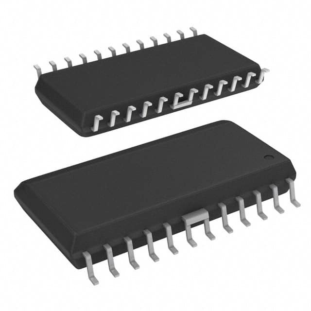
- Part No.:
- A3973SLBTR-T
- Manufacturer:
- Allegro MicroSystems
- Category:
- Motor Drivers, Controllers
- Package:
- 24-SOIC (0.295", 7.50mm Width)
- Datasheet:
-
 A3973SLBTR-T.pdf
- Description:
- IC MTR DRV BIPLR 4.5-5.5V 24SOIC
- Quantity:
- Payment:

- Shipping:

Inventory:2,404
Please send an inquiry. Send us your inquiry, and we will respond immediately.
Product details
Overview
A3973SLBTR-T from Allegro MicroSystems is a dual DMOS full-bridge PWM motor driver designed for bipolar microstepping stepper motors, supporting ±1 A continuous output current and 35 V load supply voltage. It integrates two 6-bit linear DACs for precise torque control, programmable mixed/fast/slow current-decay modes, and synchronous rectification to eliminate external clamp diodes in most applications - used in industrial CNC motion controllers and precision lab automation stages.
For engineers reviewing the A3973SLBTR-T datasheet, A3973SLBTR-T pinout, A3973SLBTR-T application, or A3973SLBTR-T equivalent, key selection considerations include its 24-pin SOICW-LB package with four internally fused leads, serial 3-wire interface (CLOCK/DATA/STROBE), internal 4 MHz oscillator, 2 V precision reference, and thermal shutdown at 165°C with 15°C hysteresis.
Technical Context
The A3973SLBTR-T implements fixed-off-time PWM current regulation using two independent 6-bit DACs (each controlling one H-bridge), with selectable current decay modes (mixed, fast, slow) programmed via 19-bit serial words. Its internal oscillator (4 MHz typical) drives programmable blank time (4–12/fOSC) and off-time (1.75–63.75 μs) counters.
Synchronous rectification is configurable via two serial bits into Active, Passive, Disabled, or Low-Side-Only modes - enabling low-RDS(on) recirculation paths that reduce power dissipation by replacing external Schottky diodes. Current sensing uses dedicated SENSE1/SENSE2 inputs referenced to ground, with trip threshold ITRIP = VDAC/(Range × RS), where Range is 4 or 8 per D18 bit.
Key Specifications
| Parameter | Value and Actual Design Meaning |
|---|---|
| Output Current | ±1.0 A continuous per bridge - supports high-torque microstepping without external heatsinking in moderate-duty cycles |
| Load Supply Voltage | 15–35 V operating range - compatible with standard 24 V industrial motor rails |
| DAC Resolution | 6-bit linear (64 steps), 1.56% current increment - enables fine-grained torque tuning across full-step to 1/64 microstep modes |
| Reference Voltage | Internal 2.0 V ±30 mV - provides stable current-setpoint baseline without external reference component |
| RDS(on) | 0.54 Ω typical (source/sink) - minimizes conduction loss at 1 A, reducing thermal load on SOICW package |
| Thermal Shutdown | 165°C junction temperature with 15°C hysteresis - protects against sustained overload or poor PCB thermal design |
| Serial Interface | 3-wire (CLOCK/DATA/STROBE), 19-bit word length - enables configuration of both bridges, decay modes, and oscillator settings over minimal GPIO count |
Pinout & Package
Package: 24-pin SOICW (LB) with four internally fused leads (pins 6, 7, 18, 19) for enhanced thermal dissipation; power tabs at ground potential - no electrical isolation required.
| Pin/Terminal | Circuit Role | Design Meaning |
|---|---|---|
| 1, 2, 13, 14, 23, 24 | GROUND | Dedicated ground return paths - critical for accurate current sensing and thermal stability; pins 1/2/13/14 are primary GND; 23/24 are auxiliary |
| 3 | SLEEP | Active-low hardware sleep control - forces serial register reset and disables all drivers to reduce IBB to 20 μA |
| 4 | VREG | Internally regulated supply for sink-side DMOS gates - requires 0.22 μF decoupling to ground to maintain stability |
| 5, 6, 7 | OUT 2B, LOAD SUPPLY 2, SENSE 2 | Bridge 2 output B, load supply return, and current sense input - forms complete half-bridge current path with OUT 2A (pin 8) |
| 8 | OUT 2A | Bridge 2 output A - paired with OUT 2B (pin 5) to drive one motor winding |
| 9, 10 | LOGIC SUPPLY, MUX REF | VDD (4.5–5.5 V) for logic core; MUX REF selects internal/external DAC reference source |
| 11, 12 | VDD, Dwg. PP-069-3 | VDD power input; pin 12 is NC (no connection) - not electrically bonded |
| 15, 16, 17 | OUT 1B, LOAD SUPPLY 1, SENSE 1 | Bridge 1 output B, load supply return, and current sense input - forms second independent half-bridge |
| 18, 19 | OUT 1A, STROBE | Bridge 1 output A; active-low serial write strobe - initiates latching of 19-bit shift register contents |
| 20, 21, 22 | CLOCK, DATA, VCP | Serial clock input (rising-edge triggered); serial data input; charge pump voltage output - powers high-side gate drivers |
| 23, 24 | CP1, CP2 | Charge pump capacitor connections - require 0.22 μF ceramic caps to ground for stable VCP generation |
Key Features
| Feature | Design Value |
|---|---|
| Programmable current decay modes | Mixed/fast/slow decay per bridge - optimizes torque smoothness and heat generation for specific motor inductance and step rate |
| Synchronous rectification | Four configurable modes (Active/Passive/Disabled/Low-Side-Only) - eliminates need for 4× external Schottky diodes in most designs, cutting BOM cost and board area |
| Integrated 4 MHz oscillator | On-chip timing source with ±25% tolerance - removes external crystal/clock generator, simplifying layout while supporting programmable off-time down to 1.75 μs |
| Two independent 6-bit DACs | Separate current setpoints for each H-bridge - enables asymmetric microstepping or dual-motor control from single IC |
| Thermal and UVLO protection | 165°C shutdown with 15°C hysteresis + 4.2 V VDD UVLO - prevents latch-up during power sequencing faults or thermal runaway |
Applications
| Industrial CNC Positioning | Lab Automation Stages |
|---|---|
|
Use Scenario: Closed-loop X-Y-Z stage control in semiconductor wafer inspection systems requiring sub-micron repeatability and vibration-free motion. IC Role / Device Role / Timing Role: Dual-bridge PWM driver executing microstepping commands from FPGA-based motion controller; 6-bit DACs set phase currents dynamically per step position. Use Value: Synchronous rectification reduces heat rise by >40% vs. diode-clamped designs, enabling compact enclosure design without forced air cooling. |
Use Scenario: Precision syringe pump actuation in clinical diagnostic analyzers, where smooth flow delivery avoids sample cross-contamination. IC Role / Device Role / Timing Role: Bipolar stepper driver managing two independent axes (valve positioning + plunger advance); serial interface allows real-time current profile updates during dispensing. Use Value: Programmable mixed-decay mode suppresses mid-band resonance, eliminating audible noise and mechanical vibration during low-speed operation. |
| 3D Printer Extruder Control | Medical Imaging Gantry Drive |
|
Use Scenario: High-resolution filament extrusion in desktop FDM printers, demanding consistent torque across variable load conditions and ambient temperatures. IC Role / Device Role / Timing Role: Full-bridge driver for NEMA17 stepper; internal 2 V reference and 6-bit DACs enable closed-loop current calibration without external components. Use Value: Thermal shutdown with hysteresis prevents thermal derating during extended print jobs, maintaining positional accuracy over multi-hour runs. |
Use Scenario: Rotational gantry movement in portable ultrasound systems, where EMI-sensitive analog front-end requires ultra-low switching noise. IC Role / Device Role / Timing Role: Motor driver synchronized to system clock via external OSC input; slow-decay mode selected to minimize high-frequency current transients. Use Value: 0.54 Ω RDS(on) limits conduction loss to <550 mW per bridge at 1 A, reducing conducted EMI from thermal cycling effects. |
Equivalent & Alternatives
The following parts are listed as comparable options for similar dual H-bridge PWM motor driver applications.
| Alternative Part | Technical Difference | Application Difference | Selection Advice |
|---|---|---|---|
| TB6600HG | Higher 4.5 A rating, but 40 V max; no integrated DACs - requires external current-setting DAC or resistor network | Best for high-current (>2 A) open-loop stepper systems; lacks microstepping resolution of A3973SLBTR-T's 6-bit DACs | Choose TB6600HG only when peak current exceeds ±1 A and microstepping granularity is secondary to raw torque |
| DRV8825 | 2.2 A rating, 3.3–45 V supply; built-in indexer and 1/32 microstepping - but no serial configuration interface | Suitable for simpler microcontroller-based systems where SPI/UART resources are constrained; lacks programmable decay modes | Select DRV8825 if board space is limited and fixed microstepping resolution suffices; avoid when dynamic decay-mode switching is required |
Compared with TB6600HG and DRV8825, the A3973SLBTR-T uniquely combines serial configurability, dual independent 6-bit DACs, and four synchronous rectification modes - making it optimal for applications needing adaptive current profiling and EMI-sensitive layouts, despite its lower current ceiling.
Availability
A3973SLBTR-T is available at Aetrix Electronics and suitable for industrial CNC positioning, lab automation stages, 3D printer extruder control, and medical imaging gantry drive applications requiring stable component supply and long-term production continuity.
Supply support for A3973SLBTR-T includes scheduled delivery planning, volume procurement assistance, BOM continuity management, traceable sourcing, and lifecycle availability coordination for OEM customers, industrial embedded developers, connected-device designers, and electronics production programs.
Manufacturer
Allegro MicroSystems is a U.S.-based designer of high-performance magnetic sensors and power ICs, founded in 1989 and headquartered in Worcester, Massachusetts.
The A3973 product line targets precision motion control in industrial and medical equipment, emphasizing integrated current regulation, thermal robustness, and flexible microstepping implementation without external timing components.
FAQ
What is the maximum continuous output current supported by the A3973SLBTR-T?
The A3973SLBTR-T supports ±1.0 A continuous output current per bridge under specified thermal conditions (TA ≤ 85°C, adequate PCB copper). This rating assumes use of the LB package's four fused leads for thermal enhancement and proper decoupling of VREG and VCP pins with 0.22 μF capacitors. Exceeding this current may trigger thermal shutdown at 165°C junction temperature.
Does the A3973SLBTR-T require an external oscillator, or does it have an internal clock source?
The A3973SLBTR-T includes a 4 MHz internal oscillator usable without external components - the OSC pin is shorted to ground in default configuration. For higher timing precision, an external clock (2.5–6.0 MHz) can be applied to the OSC pin, with internal dividers (÷1, ÷2, ÷4) selectable via serial bits D12–D13. The internal oscillator's frequency tolerance is process-dependent unless a precision resistor is added between OSC and VDD.
How does the A3973SLBTR-T implement microstepping control?
The A3973SLBTR-T achieves microstepping through two independent 6-bit linear DACs (one per H-bridge), each setting current magnitude in 1.56% increments of full scale. Combined with programmable phase bits (D13/D14) and decay-mode selection (D15/D16), it supports full-step, half-step, and fractional microstepping up to 1/64. Current levels are updated dynamically via the 3-wire serial interface without interrupting motor operation.
Can the A3973SLBTR-T operate with 3.3 V logic-level control signals?
Yes, the A3973SLBTR-T accepts 3.3 V or 5 V logic-level inputs on CLOCK, DATA, STROBE, and SLEEP pins - its logic input voltage range is –0.3 V to VDD + 0.3 V, and VDD operates from 4.5 V to 5.5 V. Input thresholds are defined at 2.0 V (logic high) and 0.8 V (logic low), ensuring reliable recognition of 3.3 V CMOS signals even with VDD = 5.0 V.
What thermal protection features are built into the A3973SLBTR-T?
The A3973SLBTR-T incorporates junction-temperature-based thermal shutdown at 165°C (typical) with 15°C hysteresis, plus undervoltage lockout (UVLO) that disables outputs if VDD drops below 3.9 V. These protections operate independently of the serial interface and remain active in sleep mode. No special power-up sequencing is required - the device resets safely on VDD ramp-up.
A3973SLBTR-T Specifications
- Product attributes
- Attribute value
- Manufacturer:
- Allegro MicroSystems
- Series:
- -
- Package/Case:
- 24-SOIC (0.295", 7.50mm Width)
- Packaging:
- Tape & Reel (TR)
- Product Status:
- Obsolete
- Motor Type - Stepper:
- Bipolar
- Motor Type - AC, DC:
- -
- Function:
- Driver - Fully Integrated, Control and Power Stage
- Output Configuration:
- Half Bridge (4)
- Interface:
- Serial
- Technology:
- DMOS
- Step Resolution:
- 1 ~ 1/64
- Applications:
- General Purpose
- Current - Output:
- 1A
- Voltage - Supply:
- 4.5V ~ 5.5V
- Voltage - Load:
- 15V ~ 35V
- Operating Temperature:
- -20°C ~ 150°C (TJ)
- Grade:
- -
- Qualification:
- -
- Mounting Type:
- Surface Mount
- Supplier Device Package:
- 24-SOIC
A3973SLBTR-T FAQ
1.How can I place an order for A3973SLBTR-T through Aetrix?
Please submit a Request for Quotation (RFQ) for A3973SLBTR-T on Aetrix. Our sales agent will provide a competitive quotation and guide you through the order confirmation once you accept the terms.
2.Are the price and stock information for A3973SLBTR-T reliable?
The price and inventory of A3973SLBTR-T are updated periodically and may fluctuate due to market conditions. Stock and pricing data are typically refreshed every 24 hours. Quotation validity for A3973SLBTR-T is usually 5 days.
3.What payment methods are accepted for A3973SLBTR-T?
We accept Wire Transfer, PayPal, Credit Card, Western Union, MoneyGram, and Escrow for A3973SLBTR-T transactions.
Note: Certain payment methods may incur a processing fee.
4.How is shipping managed for A3973SLBTR-T?
A3973SLBTR-T orders can be shipped via leading logistics carriers, including DHL, UPS, FedEx, TNT, or Registered Mail.
Once your A3973SLBTR-T order is processed, you will receive an email with the shipment details and tracking number.
Note: Tracking information may take up to 24 hours to appear. Express delivery typically takes 3–5 business days.
5.How can I obtain technical support or documentation for A3973SLBTR-T?
For technical support, including A3973SLBTR-T datasheets, pinout diagrams, or application guidance, please contact our engineering support team. They can provide detailed documentation and assistance for your A3973SLBTR-T requirements.
6.How does Aetrix verify that A3973SLBTR-T is sourced from the original manufacturer or authorized distributors?
All A3973SLBTR-T products on Aetrix are procured from qualified distributors and authorized channels. Our dedicated quality assurance team conducts strict verification, including traceability checks and, if necessary, third-party testing. This ensures that A3973SLBTR-T meets industry standards.
7.What is the process for return or replacement of A3973SLBTR-T?
All A3973SLBTR-T units undergo pre-shipment inspection (PSI). If there is an issue with A3973SLBTR-T, returns or replacements are accepted under the following conditions:
1.Quantity discrepancies, incorrect items, or visible external defects (such as breakage or corrosion), acknowledged by Aetrix.
2.The issue is reported within 90 days of delivery.
3.The A3973SLBTR-T part is unused and in its original packaging.
Return procedure for A3973SLBTR-T:
1.Submit a request within 90 days.
2.Obtain a Return Material Authorization (RMA) from Aetrix.
A3973SLBTR-T Tags

-
DRV2603RUNR
Texas Instruments

-
DRV8837CDSGR
Texas Instruments

-
DRV8837DSGR
Texas Instruments
-
DRV8838DSGR
Texas Instruments

-
DRV8839DSSR
Texas Instruments

-
EMC2301-1-ACZL-TR
Microchip Technology
-
DRV8231ADSGR
Texas Instruments

-
EMC2302-2-AIZL-TR
Microchip Technology

-
DRV8800PWPR
Texas Instruments
-
DRV8835DSSR
Texas Instruments

-
EMC2303-1-KP-TR
Microchip Technology

-
DRV8876PWPR
Texas Instruments
Tech Hub

A practical engineering and sourcing framework covering lifecycle verification, lifetime-buy calculations, replacement qualification, supplier checks and counterfeit-risk controls.

TTL and CMOS logic families differ in thresholds, loading, output drive, power and timing. This engineering guide compares 74HC and 74HCT, calculates noise margins and checks 3.3 V/5 V compatibility.

A practical engineering guide to 3.3V and 5V logic compatibility, input thresholds, resistor dividers, translator ICs, MOSFET level shifting, I2C pull-ups, timing limits and power-sequencing risks.

The 74HC595 uses push-pull logic outputs, while the TPIC6B595 uses 50 V open-drain DMOS sinks for higher-power loads. This guide compares timing, current limits, 3.3 V interfacing, load wiring, thermal…

The 74HC595 converts serial data into eight stable parallel outputs. This guide covers pin functions, shift and storage timing, OE and MR behavior, drive-current limits, cascading, voltage compatibilit…

A technical comparison of level-sensitive latches and edge-triggered flip-flops, covering timing windows, setup and hold limits, master–slave operation, time borrowing, race-through, HDL inference and…

A D latch stores one bit while Enable controls when data can pass. This reference covers gate-level operation, truth tables, transparency, setup and hold timing, LE versus OE, common ICs and practical …

An SR latch stores one bit through cross-coupled feedback. This engineering reference covers NOR and NAND implementations, truth tables, forbidden-state recovery, gated operation, switch debouncing, fa…

Latch circuits retain one bit through feedback. This technical reference covers SR and D latches, truth tables, transparency, timing limits, latch-versus-flip-flop behavior, applications and common log…

An engineering guide to LED driver operation, constant-current and constant-voltage outputs, linear and switching topologies, dimming, IC selection, calculations, replacement compatibility, and fault c…


