
 My Inquiry
 My Account


Allegro MicroSystems A3983SLP
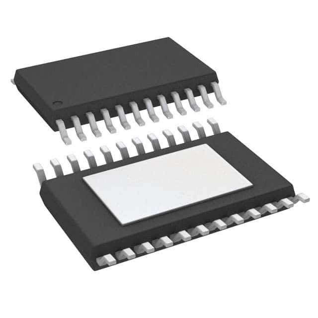
- Part No.:
- A3983SLP
- Manufacturer:
- Allegro MicroSystems
- Category:
- Motor Drivers, Controllers
- Package:
- 24-TSSOP (0.173", 4.40mm Width) Exposed Pad
- Datasheet:
-
 A3983SLP.pdf
- Description:
- IC MTR DRV BIPOLR 3-5.5V 24TSSOP
- Quantity:
- Payment:

- Shipping:

Inventory:4,104
Please send an inquiry. Send us your inquiry, and we will respond immediately.
Product details
Overview
A3983SLP from Allegro MicroSystems is a DMOS bipolar stepper motor driver IC with integrated translator, designed for full-, half-, quarter-, and eighth-step microstepping control of up to ±2 A per phase at 35 V supply. It features automatic mixed/slow decay mode selection, synchronous rectification, and fixed off-time PWM current regulation. Used in precision motion control systems such as medical pumps and automated lab equipment.
For engineers reviewing the A3983SLP datasheet, A3983SLP pinout, A3983SLP application, or A3983SLP equivalent, key selection criteria include its 24-pin TSSOP-LP package with exposed thermal pad, 30 μs typical fixed off-time, ±2 A output drive, VREF-based current programming, and translator-enabled single-pulse step interface.
Technical Context
The A3983SLP implements dual N-channel DMOS full-bridge outputs with independent current regulation per phase using external sense resistors (RS1/RS2) and a DAC-controlled trip threshold derived from VREF. Its translator interprets STEP/DIR/MS1/MS2 inputs to sequence microstep current profiles without external sequencing logic.
Chopping control dynamically selects Slow or Mixed decay based on direction of current change per phase - Slow decay for increasing current, Mixed decay (31.25% fast + remainder slow) for decreasing current - reducing audible noise and improving step accuracy. Synchronous rectification minimizes power dissipation by replacing body diode conduction with low-RDS(ON) FET switching during decay.
Key Specifications
| Parameter | Value and Actual Design Meaning |
|---|---|
| Output Drive | ±2 A per phase, enabling direct driving of mid-power bipolar stepper motors without external amplification |
| Supply Voltage | 8–35 V motor supply (VBB), 3.0–5.5 V logic supply (VDD), supporting wide-range industrial DC bus operation |
| Microstep Resolution | Full/half/quarter/eighth-step via MS1/MS2 logic inputs - no firmware or complex timing required |
| Fixed Off-Time | 20–40 μs (typ. 30 μs), set by ROSC resistor or VDD tie, determining minimum PWM switching period and current ripple |
| Sense Voltage Limit | 0.5 V max on SENSE1/SENSE2 pins - constrains minimum sense resistor value for ±2 A operation |
| Thermal Protection | Thermal shutdown at 165°C with 15°C hysteresis, plus UVLO (2.7 V enable threshold) and crossover-current protection |
| RDS(ON) | 0.30–0.45 Ω (sink/source), minimizing conduction loss and heat generation at rated load currents |
Pinout & Package
Package: 24-pin TSSOP with exposed thermal pad (suffix LP), 7.80 × 4.40 mm footprint, 1.2 mm max height, lead-free with 100% matte tin plating. Thermal pad must be soldered to PCB ground plane with thermal vias for RθJA = 28°C/W performance.
| Pin/Terminal | Circuit Role | Design Meaning |
|---|---|---|
| CP1, CP2 | Charge pump terminals | Support gate drive voltage > VBB for high-side N-channel DMOS; require 0.1 μF ceramic capacitor between them |
| VCP | Charge pump reservoir | Must connect 0.1 μF ceramic capacitor to VBB to stabilize high-side gate drive during PWM |
| VREG | Internal regulator output | Supplies sink-side DMOS gates; requires 0.22 μF ceramic decoupling to ground |
| MS1, MS2 | Microstep resolution select | Set step mode (full/half/quarter/eighth); MS2 has internal 100 kΩ pull-down |
| STEP, DIR, RESET, ENABLE, SLEEP | Digital control inputs | CMOS-compatible (3.0–5.5 V), with 150–500 mV hysteresis; all except RESET affect operation on next rising edge |
| OUT1A/OUT1B, OUT2A/OUT2B | DMOS full-bridge outputs | Drive two motor phases; each pair forms H-bridge with ±2 A capability and crossover-current protection |
| SENSE1, SENSE2 | Current sense inputs | Monitor voltage across external RS1/RS2 resistors; absolute max 0.5 V - limits min RS to 0.25 Ω at ±2 A |
| VBB1, VBB2 | Motor supply inputs | Independent high-voltage rails for each bridge; support up to 35 V with internal UVLO monitoring |
| GND (pins 13, 24 + PAD) | Ground reference | Multiple GND pins and exposed thermal pad must be connected to single-point star ground under device |
Key Features
| Feature | Design Value |
|---|---|
| Integrated translator | Eliminates need for external step-sequence logic or microcontroller firmware - one STEP pulse = one microstep |
| Automatic decay mode selection | Dynamically chooses Slow or Mixed decay per phase based on current direction change, reducing distortion and noise |
| Synchronous rectification | Replaces body diode conduction with active FET switching during decay, cutting power dissipation vs. asynchronous designs |
| Low RDS(ON) DMOS outputs | 0.30–0.45 Ω enables ±2 A drive with <1.5 W conduction loss per bridge at full load |
| Comprehensive protection | Includes thermal shutdown (165°C), UVLO (2.7 V), and crossover-current detection - no external fault management needed |
Applications
| Medical Infusion Pumps | Industrial CNC Positioning |
|---|---|
|
Use Scenario: Precise, quiet, repeatable fluid delivery in portable and hospital-grade infusion devices. IC Role / Device Role / Timing Role: Translator-driven microstepping driver controlling 2-phase bipolar stepper motor for syringe actuation. Use Value: Eighth-step resolution and automatic decay selection ensure smooth, low-vibration flow control without audible motor whine. |
Use Scenario: Open-loop positioning of tooling stages in compact benchtop CNC mills and engravers. IC Role / Device Role / Timing Role: Standalone stepper driver interfacing directly to FPGA or simple MCU GPIOs for motion control. Use Value: Single-pulse STEP interface and built-in current regulation reduce host processor overhead and eliminate external current-sense amplifiers. |
| Automated Laboratory Analyzers | 3D Printer Extruder Control |
|
Use Scenario: Reagent dispensing and sample carousel indexing requiring high positional repeatability and ESD robustness. IC Role / Device Role / Timing Role: Bipolar stepper driver managing multi-axis sample handling with thermal and UVLO fault resilience. Use Value: Integrated protection and 35 V VBB headroom support 24 V industrial power rails while maintaining safe operation during brownouts. |
Use Scenario: Compact, cost-sensitive extruder motor control in consumer-grade fused deposition modeling (FDM) printers. IC Role / Device Role / Timing Role: Low-profile TSSOP-LP driver enabling dense PCB layouts and efficient thermal management via exposed pad. Use Value: 24-pin TSSOP-LP package with thermal vias achieves 28°C/W junction-to-ambient, allowing sustained ±2 A operation without heatsinks. |
Equivalent & Alternatives
The following parts are listed as comparable options for similar stepper motor driver applications.
| Alternative Part | Technical Difference | Application Difference | Selection Advice |
|---|---|---|---|
| TB6600HG | Higher 4.5 A rating, external oscillator, no integrated translator - requires step/direction sequencing logic | Better suited for high-torque motors but increases system complexity and BOM count | Choose TB6600HG only when >±2 A drive or custom decay control is required; A3983SLP offers simpler integration |
| DRV8825 | Lower 2.2 A rating, 3.3–5.5 V logic, integrated translator, but no synchronous rectification or automatic decay selection | Compatible with 3.3 V controllers but lacks dynamic decay optimization for low-noise operation | Prefer DRV8825 for 3.3 V systems where thermal margin is ample; A3983SLP delivers superior acoustic performance in noise-sensitive environments |
Compared with TB6600HG and DRV8825, the A3983SLP uniquely combines translator simplicity, automatic decay adaptation, and synchronous rectification - delivering lower audible noise, higher step accuracy, and reduced power dissipation in space-constrained 24 V industrial motion systems.
Availability
A3983SLP is available at Aetrix Electronics and suitable for medical infusion pumps, industrial CNC positioning, automated laboratory analyzers, and 3D printer extruder control requiring stable component supply and long-term production continuity.
Supply support for A3983SLP includes scheduled delivery planning, volume procurement assistance, BOM continuity management, traceable sourcing, and lifecycle availability coordination for OEM customers, industrial embedded developers, connected-device designers, and electronics production programs.
Manufacturer
Allegro MicroSystems is a U.S.-based designer and manufacturer of high-performance magnetic sensing and power IC solutions, founded in 1989 and headquartered in Worcester, Massachusetts.
The A3983 belongs to Allegro's DMOS stepper driver product line, engineered specifically for cost-sensitive, space-constrained motion control applications requiring integrated translation, robust protection, and minimal external components.
FAQ
What is the maximum motor supply voltage supported by the A3983SLP?
The A3983SLP supports a motor supply voltage (VBB) up to 35 V, with absolute maximum rating specified at 35 V. Operation above 35 V risks permanent damage. The device maintains full functionality across 8–35 V, making it suitable for 12 V, 24 V, and 32 V industrial DC bus systems. Always observe the 0.5 V maximum sense voltage limit when sizing current-sense resistors for high-VBB operation.
How does the A3983SLP determine whether to use Slow or Mixed decay mode?
The A3983SLP determines decay mode per phase by comparing the DAC output level before and after each STEP input. If the new DAC level is higher, Slow decay is selected; if lower, Mixed decay (31.25% fast decay followed by slow decay) is used. This real-time decision occurs independently for each full-bridge and is implemented entirely in hardware - no software or configuration is required. The A3983SLP datasheet confirms this behavior in the Functional Description section.
Can the A3983SLP operate with a 3.3 V logic supply?
Yes, the A3983SLP accepts a logic supply (VDD) from 3.0 V to 5.5 V, so 3.3 V operation is fully supported and within specification. Input thresholds scale with VDD (e.g., VIN(1) ≥ 0.7×VDD), ensuring reliable logic-level recognition. However, VCP and charge pump operation depend on VBB, not VDD - so motor supply must still meet minimum 8 V requirement regardless of logic voltage. The A3983SLP electrical characteristics table explicitly lists 3.0 V as the minimum VDD.
What is the purpose of the exposed thermal pad on the A3983SLP package?
The exposed thermal pad on the A3983SLP's 24-pin TSSOP-LP package provides a low-thermal-resistance path from the die to the PCB ground plane. When soldered directly to a copper area with thermal vias, it reduces RθJA to 28°C/W (per JEDEC 4-layer board standard), enabling continuous ±2 A operation without external heatsinking. The pad must be connected to GND (pins 13 and 24) externally - failure to do so risks thermal runaway and premature device failure. The A3983SLP package drawing and Application Layout section detail required PCB land pattern and via placement.
Does the A3983SLP require external Schottky diodes for flyback protection?
No, the A3983SLP does not require external Schottky diodes due to its integrated synchronous rectification feature. During current decay, the IC actively turns on appropriate low-RDS(ON) DMOS FETs to recirculate motor current, bypassing body diodes and reducing power loss. This eliminates conduction losses associated with external diodes and simplifies layout. The A3983SLP datasheet states: "synchronous rectification … can eliminate the need for external Schottky diodes in many applications."
A3983SLP Specifications
- Product attributes
- Attribute value
- Manufacturer:
- Allegro MicroSystems
- Series:
- -
- Package/Case:
- 24-TSSOP (0.173", 4.40mm Width) Exposed Pad
- Packaging:
- Tube
- Product Status:
- Obsolete
- Motor Type - Stepper:
- Bipolar
- Motor Type - AC, DC:
- -
- Function:
- Driver - Fully Integrated, Control and Power Stage
- Output Configuration:
- Half Bridge (4)
- Interface:
- Logic
- Technology:
- DMOS
- Step Resolution:
- 1, 1/2, 1/4, 1/8
- Applications:
- General Purpose
- Current - Output:
- 2A
- Voltage - Supply:
- 3V ~ 5.5V
- Voltage - Load:
- 8V ~ 35V
- Operating Temperature:
- -20°C ~ 150°C (TJ)
- Grade:
- -
- Qualification:
- -
- Mounting Type:
- Surface Mount
- Supplier Device Package:
- 24-TSSOP-EP
A3983SLP FAQ
1.How can I place an order for A3983SLP through Aetrix?
Please submit a Request for Quotation (RFQ) for A3983SLP on Aetrix. Our sales agent will provide a competitive quotation and guide you through the order confirmation once you accept the terms.
2.Are the price and stock information for A3983SLP reliable?
The price and inventory of A3983SLP are updated periodically and may fluctuate due to market conditions. Stock and pricing data are typically refreshed every 24 hours. Quotation validity for A3983SLP is usually 5 days.
3.What payment methods are accepted for A3983SLP?
We accept Wire Transfer, PayPal, Credit Card, Western Union, MoneyGram, and Escrow for A3983SLP transactions.
Note: Certain payment methods may incur a processing fee.
4.How is shipping managed for A3983SLP?
A3983SLP orders can be shipped via leading logistics carriers, including DHL, UPS, FedEx, TNT, or Registered Mail.
Once your A3983SLP order is processed, you will receive an email with the shipment details and tracking number.
Note: Tracking information may take up to 24 hours to appear. Express delivery typically takes 3–5 business days.
5.How can I obtain technical support or documentation for A3983SLP?
For technical support, including A3983SLP datasheets, pinout diagrams, or application guidance, please contact our engineering support team. They can provide detailed documentation and assistance for your A3983SLP requirements.
6.How does Aetrix verify that A3983SLP is sourced from the original manufacturer or authorized distributors?
All A3983SLP products on Aetrix are procured from qualified distributors and authorized channels. Our dedicated quality assurance team conducts strict verification, including traceability checks and, if necessary, third-party testing. This ensures that A3983SLP meets industry standards.
7.What is the process for return or replacement of A3983SLP?
All A3983SLP units undergo pre-shipment inspection (PSI). If there is an issue with A3983SLP, returns or replacements are accepted under the following conditions:
1.Quantity discrepancies, incorrect items, or visible external defects (such as breakage or corrosion), acknowledged by Aetrix.
2.The issue is reported within 90 days of delivery.
3.The A3983SLP part is unused and in its original packaging.
Return procedure for A3983SLP:
1.Submit a request within 90 days.
2.Obtain a Return Material Authorization (RMA) from Aetrix.
A3983SLP Tags

-
DRV2603RUNR
Texas Instruments

-
DRV8837CDSGR
Texas Instruments

-
DRV8837DSGR
Texas Instruments
-
DRV8838DSGR
Texas Instruments

-
DRV8839DSSR
Texas Instruments

-
EMC2301-1-ACZL-TR
Microchip Technology
-
DRV8231ADSGR
Texas Instruments

-
EMC2302-2-AIZL-TR
Microchip Technology

-
DRV8800PWPR
Texas Instruments
-
DRV8835DSSR
Texas Instruments

-
EMC2303-1-KP-TR
Microchip Technology

-
DRV8876PWPR
Texas Instruments
Tech Hub

A practical engineering and sourcing framework covering lifecycle verification, lifetime-buy calculations, replacement qualification, supplier checks and counterfeit-risk controls.

TTL and CMOS logic families differ in thresholds, loading, output drive, power and timing. This engineering guide compares 74HC and 74HCT, calculates noise margins and checks 3.3 V/5 V compatibility.

A practical engineering guide to 3.3V and 5V logic compatibility, input thresholds, resistor dividers, translator ICs, MOSFET level shifting, I2C pull-ups, timing limits and power-sequencing risks.

The 74HC595 uses push-pull logic outputs, while the TPIC6B595 uses 50 V open-drain DMOS sinks for higher-power loads. This guide compares timing, current limits, 3.3 V interfacing, load wiring, thermal…

The 74HC595 converts serial data into eight stable parallel outputs. This guide covers pin functions, shift and storage timing, OE and MR behavior, drive-current limits, cascading, voltage compatibilit…

A technical comparison of level-sensitive latches and edge-triggered flip-flops, covering timing windows, setup and hold limits, master–slave operation, time borrowing, race-through, HDL inference and…

A D latch stores one bit while Enable controls when data can pass. This reference covers gate-level operation, truth tables, transparency, setup and hold timing, LE versus OE, common ICs and practical …

An SR latch stores one bit through cross-coupled feedback. This engineering reference covers NOR and NAND implementations, truth tables, forbidden-state recovery, gated operation, switch debouncing, fa…

Latch circuits retain one bit through feedback. This technical reference covers SR and D latches, truth tables, transparency, timing limits, latch-versus-flip-flop behavior, applications and common log…

An engineering guide to LED driver operation, constant-current and constant-voltage outputs, linear and switching topologies, dimming, IC selection, calculations, replacement compatibility, and fault c…


