
 My Inquiry
 My Account


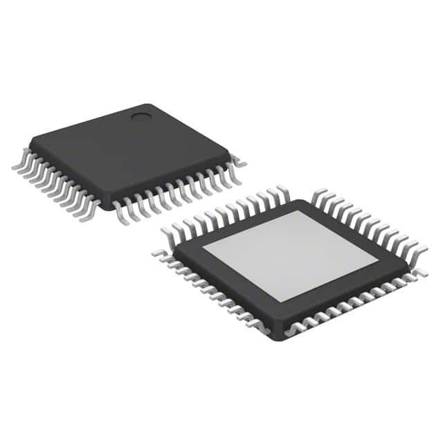
Allegro MicroSystems A4911KJPTR-T
- Part No.:
- A4911KJPTR-T
- Manufacturer:
- Allegro MicroSystems
- Category:
- Motor Drivers, Controllers
- Package:
- 48-LQFP Exposed Pad
- Datasheet:
-
 A4911KJPTR-T.pdf
- Description:
- IC MOTOR DRVR MULTIPHASE 48LQFP
- Quantity:
- Payment:

- Shipping:

Inventory:3,848
Please send an inquiry. Send us your inquiry, and we will respond immediately.
Product details
Overview
A4911KJPTR-T from Allegro MicroSystems is a three-phase N-channel MOSFET gate driver IC designed for automotive BLDC motor control, featuring programmable gate drive voltage (7.5–11.7 V), 48-pin LQFP package with exposed thermal pad, integrated current sense amplifiers (gain = 20 V/V, offset = 2.5 V), and ASIL-D-capable diagnostics. It operates across 5.5–50 V supply range and supports both logic-input and SPI-based bridge control.
For engineers reviewing the A4911KJPTR-T datasheet, A4911KJPTR-T pinout, A4911KJPTR-T application, or A4911KJPTR-T equivalent, key selection criteria include bootstrap gate drive capability for N-MOSFET bridges, adjustable dead time (1.25–2.15 µs), three independent current sense channels with programmable gain/offset, charge pump operation down to 5.5 V, and AEC-Q100 qualification for automotive powertrain systems.
Technical Context
The A4911KJPTR-T implements a dual-control architecture supporting direct logic inputs (HA/LA–HC/LC) and SPI register-based phase control, enabling block commutation or sinusoidal excitation. Its integrated charge pump regulator sustains gate drive above battery voltage down to 7 V, with top-off capability for 100% PWM duty cycle.
Three current sense amplifiers provide differential inputs (CSxP/CSxM), programmable gain (default 20 V/V), and offset output (OOS), feeding real-time motor phase current data to external controllers. Diagnostics include VDS fault monitoring (adjustable thresholds), overcurrent detection (0.8–1.08 V threshold), open-load detection, and temperature warning (125–145 °C).
Key Specifications
| Parameter | Value and Actual Design Meaning |
|---|---|
| Supply Voltage Range | 5.5 V to 50 V - supports wide automotive battery transients and cold-crank operation down to 5.5 V. |
| Gate Drive Voltage | 7.5–8.5 V (VRG = 0) or 9–11.7 V (VRG = 1) - selectable for optimized MOSFET RDS(on) and switching loss trade-offs. |
| Dead Time Programmability | 1.25–2.15 µs - prevents shoot-through in three-phase bridge by enforcing minimum off-time between high- and low-side FETs. |
| Current Sense Gain | 20 V/V (default) - provides precise 1 mV/mA scaling for shunt-based phase current measurement. |
| Thermal Resistance (RθJA) | 23 °C/W (4-layer PCB) - enables >3 W continuous power dissipation with standard automotive PCB layout. |
| Diagnostic Coverage | ASIL D-compliant diagnostics - includes VREG undervoltage, VBB UV/OV, bootstrap UV, VDS fault, overcurrent, open-load, and overtemperature detection. |
| Interface | SPI-compatible serial interface (SCK/SDI/SDO/STRn) - allows runtime reconfiguration of registers and diagnostic readback without logic pin changes. |
Pinout & Package
Package: 48-pin LQFP (7 mm × 7 mm, 1.6 mm height) with exposed thermal pad (suffix JP); RoHS-compliant, 100% matte-tin leadframe plating.
| Pin/Terminal | Circuit Role | Design Meaning |
|---|---|---|
| GHA, GHB, GHC | High-side gate drive outputs | Drive N-MOSFET gates via bootstrap capacitors (CA/CB/CC); support up to 11 Ω pull-up on-resistance at 150°C. |
| GLA, GLB, GLC | Low-side gate drive outputs | Directly sourced from VREG; 2.4 Ω typical pull-down on-resistance at 25°C ensures fast turn-off. |
| CS1P–CS3M | Differential current sense inputs | Three independent pairs for shunt resistor monitoring; ±1 mV input offset enables <10 mA sensing resolution. |
| OOS | Programmable offset output | Delivers configured VOOS (default 2.5 V) to set common-mode level for ADC interfacing. |
| HA–LC | Direct logic control inputs | TTL-compatible (VIH ≥ 2.0 V, VIL ≤ 0.8 V); enable discrete PWM or commutation state control without SPI. |
| SAL, SBL, SCL | Phase state logic outputs | Reflect real-time SA/SB/SC voltage levels for closed-loop feedback or safety monitoring. |
| DIAG | Configurable diagnostic output | Provides fault pulse (90–110 ms period), temperature analog voltage (1440 mV @ TJ = 25°C), or clock output per DG[1:0] setting. |
| VREG | Internal gate drive supply | Regulated 8 V or 11 V output powers low-side drivers and logic; stable down to VBB = 5.5 V via charge pump. |
Key Features
| Feature | Design Value |
|---|---|
| Bootstrap gate drive for N-MOSFET bridge | Enables cost-effective, high-efficiency three-phase inverter using only N-channel MOSFETs without P-channel or isolated supplies. |
| Adjustable dead time with crossover protection | Prevents shoot-through faults during phase transitions; programmable 1.25–2.15 µs delay ensures robust operation across temperature and voltage extremes. |
| Integrated current sense amplifiers (x3) | Eliminates need for external op-amps and precision resistors; 2 MHz bandwidth and 1 µs settling support high-speed FOC algorithms. |
| Charge pump + top-off for 100% PWM | Maintains high-side gate voltage during continuous conduction, enabling regenerative braking and zero-speed torque control in BLDC applications. |
| ASIL-D-capable diagnostics | Includes online verification of VBRG, LSS, and sense amp functionality via serial interface-required for ISO 26262-compliant motor control systems. |
| Automotive AEC-Q100 Grade 0 | Qualified for operation from –40°C to +150°C ambient, supporting under-hood placement in electric power steering and traction inverters. |
Applications
| Electric Power Steering (EPS) | Automotive HVAC Blower |
|---|---|
Use Scenario: Driving 3-phase BLDC motor in column-assist EPS system with torque overlay and fail-safe shutdown. IC Role / Device Role / Timing Role: Three-phase gate driver with integrated current sensing and ASIL-D diagnostics for real-time motor phase control and fault response. Use Value: Enables single-chip solution for torque ripple reduction via precise 1.25 µs dead time control and 20 V/V current gain matching shunt-based sensor accuracy. | Use Scenario: Controlling cabin air blower motor in premium vehicle HVAC system requiring quiet operation and speed regulation. IC Role / Device Role / Timing Role: Gate driver with programmable gate strength and SPI-configurable diagnostics for variable-speed fan control and thermal derating. Use Value: Reduces EMI through adjustable gate drive strength and supports 100% PWM via top-off charge pump for full-speed airflow without audible switching artifacts. |
| Onboard Charger (OBC) Auxiliary Motor | Electric Brake Booster Pump |
Use Scenario: Driving auxiliary cooling fan or pump motor in bidirectional OBC module operating in harsh thermal environments. IC Role / Device Role / Timing Role: High-reliability gate driver with VBB UV/OV protection and overtemperature shutdown (165°C junction limit) for unattended operation. Use Value: Ensures continuous thermal management during high-power charging cycles using integrated diagnostics and 23 °C/W RθJA on 4-layer PCB. | Use Scenario: Controlling vacuum pump motor in electro-hydraulic brake (EHB) system requiring functional safety and rapid fault response. IC Role / Device Role / Timing Role: Safety-certified driver with VDS fault monitoring and configurable DIAG output for ASIL-B system integration. Use Value: Delivers <110 ms fault pulse period and 20% duty cycle on DIAG for immediate MCU-level fault classification and hydraulic pressure fallback activation. |
Equivalent & Alternatives
The following parts are listed as comparable options for similar three-phase gate driver applications.
| Alternative Part | Technical Difference | Application Difference | Selection Advice |
|---|---|---|---|
| STSPIN32F0B | Integrated 32-bit ARM Cortex-M0 MCU + gate driver; no external current sense amps; 65 V max VBB. | Targeted at compact, self-contained motor control with embedded firmware; lacks independent current sense outputs and ASIL-D diagnostics. | Select when system-level integration (MCU + driver) reduces BOM count and board space is constrained. |
| DRV8305-Q1 | Separate high/low-side drivers with integrated current sense (single shared amplifier); 60 V max VBB; no charge pump for ultra-low VBB operation. | Designed for lower-cost BLDC systems where ASIL-D is not required; supports basic diagnostics but lacks online verification and VBRG monitoring. | Select when cost sensitivity outweighs need for full ASIL-D compliance and extended low-voltage operation below 7 V. |
Compared with STSPIN32F0B and DRV8305-Q1, the A4911KJPTR-T delivers dedicated high-fidelity current sensing (three independent channels), charge pump operation down to 5.5 V, and certified ASIL-D diagnostic coverage-making it optimal for safety-critical automotive powertrain actuators where functional safety and measurement integrity are non-negotiable.
Availability
A4911KJPTR-T is available at Aetrix Electronics and suitable for electric power steering, HVAC blower control, and onboard charger auxiliary motor applications requiring stable component supply, long-term automotive lifecycle support, and AEC-Q100-compliant sourcing.
Supply support for A4911KJPTR-T includes scheduled delivery planning, volume procurement assistance, BOM continuity management, traceable sourcing, and lifecycle availability coordination for OEM customers, industrial embedded developers, connected-device designers, and electronics production programs.
Manufacturer
Allegro MicroSystems is a U.S.-based semiconductor company specializing in magnetic sensing, power ICs, and motor control solutions for automotive and industrial markets.
The A4911 product line is engineered for ASIL-D-compliant three-phase motor drives in safety-critical automotive systems-including EPS, brake boosters, and thermal management-emphasizing robust gate drive, integrated diagnostics, and extended low-voltage operation.
FAQ
What is the minimum operating supply voltage for the A4911KJPTR-T?
The A4911KJPTR-T supports a functional operating range from 5.5 V to 50 V. Below 5.5 V, gate drive outputs disable and the device enters safe state. The integrated charge pump enables gate drive operation down to 5.5 V, while maintaining VREG output stability via top-off capability-critical for cold-crank scenarios in automotive systems where battery voltage dips transiently.
Does the A4911KJPTR-T support both logic-input and SPI-based control simultaneously?
No-the A4911KJPTR-T uses exclusive control modes: either direct logic inputs (HA/LA–HC/LC) or SPI register configuration, not both concurrently. Table 3 in the datasheet defines priority logic: when ENABLE = 1 and RESETn = 1, internal control signals HIx/LOx derive from either Hx/Lx pins (if serial control bits are zero) or the Control register (if pins are held low). Mixing modes risks undefined phase states and is not recommended in production designs.
How does the A4911KJPTR-T implement shoot-through protection?
The A4911KJPTR-T prevents shoot-through via hardware-enforced dead time (programmable 1.25–2.15 µs) between complementary high- and low-side gate drive transitions, plus integrated crossover control that blocks simultaneous activation. This dual-layer protection operates independently of software or SPI commands-ensuring fail-safe behavior even during communication faults or MCU lockup in safety-critical automotive applications.
Can the current sense amplifiers in the A4911KJPTR-T be used without external components?
Yes-the A4911KJPTR-T's three current sense amplifiers require only external shunt resistors on CSxP/CSxM inputs; no external gain-setting resistors or offset calibration components are needed. Gain (default 20 V/V) and output offset (default 2.5 V) are programmable via SPI Config Registers 4–5, and the OOS pin delivers the configured VOOS directly. This eliminates external op-amp circuitry and improves measurement consistency across temperature.
What thermal performance can be expected from the A4911KJPTR-T in a 4-layer PCB design?
In a JEDEC-standard 4-layer PCB layout, the A4911KJPTR-T exhibits RθJA = 23 °C/W. At 150°C maximum junction temperature and 125°C ambient, this allows ~1.09 W of continuous power dissipation (ΔT = 25°C ÷ 23 °C/W). With proper copper pour on the exposed thermal pad and inner ground/power planes, sustained gate drive loads remain within safe operating area for automotive EPS and HVAC applications.
A4911KJPTR-T Specifications
- Product attributes
- Attribute value
- Manufacturer:
- Allegro MicroSystems
- Series:
- -
- Package/Case:
- 48-LQFP Exposed Pad
- Packaging:
- Tape & Reel (TR)
- Product Status:
- Active
- Motor Type - Stepper:
- Multiphase
- Motor Type - AC, DC:
- Brushless DC (BLDC)
- Function:
- Driver - Fully Integrated, Control and Power Stage
- Output Configuration:
- Half Bridge (3)
- Interface:
- SPI
- Technology:
- NMOS
- Step Resolution:
- -
- Applications:
- -
- Current - Output:
- -
- Voltage - Supply:
- -
- Voltage - Load:
- -
- Operating Temperature:
- -40°C ~ 150°C
- Grade:
- Automotive
- Qualification:
- -
- Mounting Type:
- Surface Mount
- Supplier Device Package:
- 48-LQFP-EP (7x7)
A4911KJPTR-T FAQ
1.How can I place an order for A4911KJPTR-T through Aetrix?
Please submit a Request for Quotation (RFQ) for A4911KJPTR-T on Aetrix. Our sales agent will provide a competitive quotation and guide you through the order confirmation once you accept the terms.
2.Are the price and stock information for A4911KJPTR-T reliable?
The price and inventory of A4911KJPTR-T are updated periodically and may fluctuate due to market conditions. Stock and pricing data are typically refreshed every 24 hours. Quotation validity for A4911KJPTR-T is usually 5 days.
3.What payment methods are accepted for A4911KJPTR-T?
We accept Wire Transfer, PayPal, Credit Card, Western Union, MoneyGram, and Escrow for A4911KJPTR-T transactions.
Note: Certain payment methods may incur a processing fee.
4.How is shipping managed for A4911KJPTR-T?
A4911KJPTR-T orders can be shipped via leading logistics carriers, including DHL, UPS, FedEx, TNT, or Registered Mail.
Once your A4911KJPTR-T order is processed, you will receive an email with the shipment details and tracking number.
Note: Tracking information may take up to 24 hours to appear. Express delivery typically takes 3–5 business days.
5.How can I obtain technical support or documentation for A4911KJPTR-T?
For technical support, including A4911KJPTR-T datasheets, pinout diagrams, or application guidance, please contact our engineering support team. They can provide detailed documentation and assistance for your A4911KJPTR-T requirements.
6.How does Aetrix verify that A4911KJPTR-T is sourced from the original manufacturer or authorized distributors?
All A4911KJPTR-T products on Aetrix are procured from qualified distributors and authorized channels. Our dedicated quality assurance team conducts strict verification, including traceability checks and, if necessary, third-party testing. This ensures that A4911KJPTR-T meets industry standards.
7.What is the process for return or replacement of A4911KJPTR-T?
All A4911KJPTR-T units undergo pre-shipment inspection (PSI). If there is an issue with A4911KJPTR-T, returns or replacements are accepted under the following conditions:
1.Quantity discrepancies, incorrect items, or visible external defects (such as breakage or corrosion), acknowledged by Aetrix.
2.The issue is reported within 90 days of delivery.
3.The A4911KJPTR-T part is unused and in its original packaging.
Return procedure for A4911KJPTR-T:
1.Submit a request within 90 days.
2.Obtain a Return Material Authorization (RMA) from Aetrix.
A4911KJPTR-T Tags

-
DRV2603RUNR
Texas Instruments

-
DRV8837CDSGR
Texas Instruments

-
DRV8837DSGR
Texas Instruments
-
DRV8838DSGR
Texas Instruments

-
DRV8839DSSR
Texas Instruments

-
EMC2301-1-ACZL-TR
Microchip Technology
-
DRV8231ADSGR
Texas Instruments

-
EMC2302-2-AIZL-TR
Microchip Technology

-
DRV8800PWPR
Texas Instruments
-
DRV8835DSSR
Texas Instruments

-
EMC2303-1-KP-TR
Microchip Technology

-
DRV8876PWPR
Texas Instruments
Tech Hub

A practical engineering and sourcing framework covering lifecycle verification, lifetime-buy calculations, replacement qualification, supplier checks and counterfeit-risk controls.

TTL and CMOS logic families differ in thresholds, loading, output drive, power and timing. This engineering guide compares 74HC and 74HCT, calculates noise margins and checks 3.3 V/5 V compatibility.

A practical engineering guide to 3.3V and 5V logic compatibility, input thresholds, resistor dividers, translator ICs, MOSFET level shifting, I2C pull-ups, timing limits and power-sequencing risks.

The 74HC595 uses push-pull logic outputs, while the TPIC6B595 uses 50 V open-drain DMOS sinks for higher-power loads. This guide compares timing, current limits, 3.3 V interfacing, load wiring, thermal…

The 74HC595 converts serial data into eight stable parallel outputs. This guide covers pin functions, shift and storage timing, OE and MR behavior, drive-current limits, cascading, voltage compatibilit…

A technical comparison of level-sensitive latches and edge-triggered flip-flops, covering timing windows, setup and hold limits, master–slave operation, time borrowing, race-through, HDL inference and…

A D latch stores one bit while Enable controls when data can pass. This reference covers gate-level operation, truth tables, transparency, setup and hold timing, LE versus OE, common ICs and practical …

An SR latch stores one bit through cross-coupled feedback. This engineering reference covers NOR and NAND implementations, truth tables, forbidden-state recovery, gated operation, switch debouncing, fa…

Latch circuits retain one bit through feedback. This technical reference covers SR and D latches, truth tables, transparency, timing limits, latch-versus-flip-flop behavior, applications and common log…

An engineering guide to LED driver operation, constant-current and constant-voltage outputs, linear and switching topologies, dimming, IC selection, calculations, replacement compatibility, and fault c…


