
 My Inquiry
 My Account


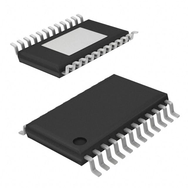
Allegro MicroSystems A4939KLPTR-T
- Part No.:
- A4939KLPTR-T
- Manufacturer:
- Allegro MicroSystems
- Category:
- Motor Drivers, Controllers
- Package:
- 28-TSSOP (0.173", 4.40mm Width) Exposed Pad
- Datasheet:
-
 A4939KLPTR-T.pdf
- Description:
- IC MTR DRV MULTI 5.5-50V 28TSSOP
- Quantity:
- Payment:

- Shipping:

Inventory:1,029
Please send an inquiry. Send us your inquiry, and we will respond immediately.
Product details
Overview
A4939KLPTR-T from Allegro MicroSystems is a three-phase N-channel MOSFET gate driver IC designed for automotive motor control, delivering regulated 13 V gate drive down to 5.5 V battery supply, integrated crossover protection, and per-phase VDS short-circuit detection with programmable threshold via VDSTH pin. It supports electronic power steering (EPS) and engine cooling fan applications.
For engineers reviewing the A4939KLPTR-T datasheet, A4939KLPTR-T pinout, A4939KLPTR-T application, or A4939KLPTR-T equivalent, key selection considerations include its 28-pin TSSOP-LP package with exposed thermal pad, Sleep mode capability (enabled), absence of on-chip LDO regulator, 5.5–50 V wide input range, and six independent TTL-compatible logic inputs for external commutation control.
Technical Context
The A4939KLPTR-T implements a charge-pump-based gate drive supply (VREG) that maintains >10 V high-side gate voltage down to 7 V VBB and sustains functional operation at 5.5 V with reduced drive. Its six gate drivers are split into three high-side (GHA/GHB/GHC) and three low-side (GLA/GLB/GLC) outputs, each controlled by dedicated logic inputs (AHI/ALO/BHI/BLO/CHI/CLO) with internal cross-conduction lockout.
Motor phase fault detection uses per-MOSFET drain-source voltage monitoring referenced to programmable VDSTH (0.2–2.0 V range), with short-to-supply and short-to-ground reporting consolidated onto a single open-drain FAULT output. Thermal protection triggers at 170–180 °C junction temperature with 15 °C hysteresis, and undervoltage lockout operates on VREG (7.25–8.5 V trip).
Key Specifications
| Parameter | Value and Actual Design Meaning |
|---|---|
| VBB Supply Range | 5.5 V to 50 V - enables operation across cold-crank (5.5 V) to load-dump (50 V) automotive transients |
| VREG Output | 12.5–13.75 V @ IREG ≤ 15 mA - powers low-side drivers and charges bootstrap capacitors for high-side N-MOSFETs |
| Gate Drive On-Resistance | RDS(on)UP = 5–13 Ω (high-side), RDS(on)DN = 1.5–4.6 Ω (low-side) - ensures fast switching with <35 ns turn-on and <20 ns turn-off times |
| Sleep Mode Current | <15 µA @ VBB = 12 V - reduces quiescent draw during vehicle standby without disabling diagnostics |
| Fault Reporting | Single open-drain FAULT pin - latches no faults but signals overtemperature, VREG UVLO, and VDS shorts simultaneously |
| VDSTH Programming | 0.2–2.0 V analog input - sets per-phase MOSFET short-circuit detection threshold with ±100 mV offset tolerance |
| Thermal Resistance | RθJA = 28 °C/W (4-layer PCB) - supports 165 °C max junction temperature in LP package with exposed thermal pad |
Pinout & Package
Package: 28-pin TSSOP with exposed thermal pad (LP), Pb-free, 100% matte-tin leadframe plating.
| Pin | Circuit Role | Design Meaning |
|---|---|---|
| LSS (1) | Low-side source return | Common source node for all three low-side MOSFETs; provides discharge path for gate capacitance |
| GLC (2) | Phase C low-side gate drive | Drives gate of N-MOSFET in bottom leg of phase C bridge; referenced to LSS |
| GHC (3) | Phase C high-side gate drive | Drives gate of N-MOSFET in top leg of phase C bridge; floating output referenced to SC |
| SC (4) | Phase C motor connection | Connects to motor winding C; serves as bootstrap capacitor negative terminal and VDS sense node |
| CC (5) | Phase C bootstrap capacitor | Positive terminal of bootstrap cap for phase C high-side drive; charges when SC pulled low |
| GLB (6) | Phase B low-side gate drive | Drives gate of N-MOSFET in bottom leg of phase B bridge; referenced to LSS |
| GHB (7) | Phase B high-side gate drive | Drives gate of N-MOSFET in top leg of phase B bridge; floating output referenced to SB |
| SB (8) | Phase B motor connection | Connects to motor winding B; serves as bootstrap capacitor negative terminal and VDS sense node |
| CB (9) | Phase B bootstrap capacitor | Positive terminal of bootstrap cap for phase B high-side drive; charges when SB pulled low |
| GLA (10) | Phase A low-side gate drive | Drives gate of N-MOSFET in bottom leg of phase A bridge; referenced to LSS |
| GHA (11) | Phase A high-side gate drive | Drives gate of N-MOSFET in top leg of phase A bridge; floating output referenced to SA |
| SA (12) | Phase A motor connection | Connects to motor winding A; serves as bootstrap capacitor negative terminal and VDS sense node |
| CA (13) | Phase A bootstrap capacitor | Positive terminal of bootstrap cap for phase A high-side drive; charges when SA pulled low |
| VREG (14) | Regulated gate drive supply | 13 V output powering low-side drivers and charging all bootstrap capacitors |
| CP2 (15) | Charge pump capacitor | Second terminal of 470 nF pump capacitor (with CP1); enables boost regulation below 16 V VBB |
| CP1 (16) | Charge pump capacitor | First terminal of 470 nF pump capacitor (with CP2); forms charge pump oscillator with internal circuitry |
| VBB (17) | Main power supply | Primary 5.5–50 V battery input powering all internal functions including logic, charge pump, and drivers |
| VBRG (18) | High-side bridge voltage sense | Monitors voltage at high-side MOSFET drains to enable accurate VDS measurement |
| GND (19) | Ground reference | Common analog/digital/power ground; must be low-impedance connection to system ground plane |
| VDDM (20) | Logic monitor input | Undervoltage monitor input (2.45–2.85 V trip); pulls down internally at 60 kΩ; disables gate drive if <1.5 V |
| VDSTH (21) | VDS threshold programming | Analog input setting short-circuit detection level (0.2–2.0 V); high-impedance, supports resistive divider |
| FAULT (22) | Diagnostic output | Open-drain active-high fault signal; requires external pull-up to ≤5.5 V; asserts on overtemp, UVLO, or VDS fault |
| AHI (23) | Phase A high-side control | TTL-compatible input (VIH ≥ 2.0 V); high = enable GHA; internal lockout prevents simultaneous AHI/ALO high |
| ALO (24) | Phase A low-side control | TTL-compatible input (VIL ≤ 0.8 V); high = enable GLA; internal lockout prevents simultaneous AHI/ALO high |
| BHI (25) | Phase B high-side control | TTL-compatible input controlling GHB; same lockout and timing behavior as AHI |
| BLO (26) | Phase B low-side control | TTL-compatible input controlling GLB; same lockout and timing behavior as ALO |
| CHI (27) | Phase C high-side control | TTL-compatible input controlling GHC; same lockout and timing behavior as AHI |
| CLO (28) | Phase C low-side control | TTL-compatible input controlling GLC; same lockout and timing behavior as ALO |
Key Features
| Feature | Design Value |
|---|---|
| Charge-pump gate drive regulation | Maintains >10 V gate voltage down to 7 V VBB; extends functional operation to 5.5 V with reduced drive |
| Per-phase VDS short-circuit detection | Programmable threshold (0.2–2.0 V) with ±100 mV offset tolerance and 1.5–4.5 µs blanking time |
| Integrated crossover protection | Hardware lockout prevents simultaneous high-side and low-side activation in any phase |
| Automotive-grade thermal management | Overtemperature warning at 170–180 °C with 15 °C hysteresis and 165 °C absolute max junction rating |
| Low-power Sleep mode | Reduces current to <15 µA while retaining fault monitoring and enabling wake-up via any logic input |
Applications
| Electronic Power Steering (EPS) | Engine Cooling Fan |
|---|---|
|
Use Scenario: High-reliability 3-phase BLDC motor control in safety-critical steering assist systems requiring ASIL-B compliance support. IC Role / Device Role / Timing Role: Gate driver providing isolated high-side/low-side control with real-time VDS fault detection and thermal shutdown. Use Value: Enables fail-safe motor disable within microseconds of short-circuit detection, meeting ISO 26262 diagnostic coverage requirements. |
Use Scenario: PWM-controlled radiator fan driving under wide battery voltage range (5.5–50 V) including cold-crank and load-dump conditions. IC Role / Device Role / Timing Role: Three-phase gate driver interfacing microcontroller PWM outputs to external N-MOSFET half-bridges. Use Value: Charge-pump regulation ensures consistent gate drive strength across full automotive voltage range, minimizing torque ripple. |
| Hydraulic Pump Actuation | Gearbox Actuator |
|
Use Scenario: Closed-loop pressure control in electro-hydraulic power steering pumps using sensorless BLDC commutation. IC Role / Device Role / Timing Role: High-current gate driver supporting external MOSFETs with fast propagation delay matching (≤10 ns phase-to-phase). Use Value: Tight propagation delay matching ensures precise timing alignment across phases, critical for smooth torque delivery and acoustic noise reduction. |
Use Scenario: Compact, thermally constrained gearbox position actuators requiring high efficiency and fault resilience. IC Role / Device Role / Timing Role: Motor driver with integrated diagnostics (VDS, overtemp, UVLO) and low-quiescent Sleep mode for parked-state power savings. Use Value: Sleep mode draws <15 µA while maintaining fault monitoring, extending battery life in always-on vehicle architectures. |
Equivalent & Alternatives
The following parts are listed as comparable options for similar three-phase gate driver applications.
| Alternative Part | Technical Difference | Application Difference | Selection Advice |
|---|---|---|---|
| MP6532GQ-Z | No integrated charge pump; requires external 12 V bias supply for high-side drive; lacks programmable VDS threshold | Suitable for non-automotive industrial BLDC drives where battery voltage stays >10 V | Select when external bias rail is available and VDS fault granularity is not required |
| DRV8305PAPR | Includes integrated 3.3 V LDO regulator and current-sense amplifiers; higher quiescent current (3 mA vs. 15 µA) | Better suited for applications needing on-chip current sensing and logic supply, but less optimal for ultra-low-power Sleep mode | Select when system-level integration (LDO + current sense) outweighs Sleep mode current advantage |
Compared with MP6532GQ-Z and DRV8305PAPR, the A4939KLPTR-T uniquely combines automotive-grade wide-input operation (5.5 V), ultra-low Sleep current (<15 µA), and programmable per-phase short-circuit detection-making it optimal for EPS and other ASIL-relevant systems requiring both fault precision and standby efficiency.
Availability
A4939KLPTR-T is available at Aetrix Electronics and suitable for electronic power steering (EPS), engine cooling fan, and hydraulic pump applications requiring stable component supply, automotive qualification, and long-term lifecycle support.
Supply support for A4939KLPTR-T includes scheduled delivery planning, volume procurement assistance, BOM continuity management, traceable sourcing, and lifecycle availability coordination for OEM customers, industrial embedded developers, connected-device designers, and electronics production programs.
Manufacturer
Allegro MicroSystems is a U.S.-based semiconductor company specializing in magnetic sensing, power ICs, and motor driver solutions for automotive and industrial markets.
The A4939 product line delivers robust three-phase gate drivers optimized for automotive BLDC motor control, emphasizing fault resilience, wide battery voltage operation, and thermal survivability in under-hood environments.
FAQ
What is the minimum battery voltage at which A4939KLPTR-T maintains full gate drive performance?
The A4939KLPTR-T maintains full (>10 V) gate drive performance down to 7 V VBB using its internal charge pump regulator. Below 7 V, functional operation continues down to 5.5 V VBB but with reduced gate drive voltage, as specified in the Electrical Characteristics table under VBB Functional Operating Range.
Does A4939KLPTR-T include an integrated LDO regulator?
No, the A4939KLPTR-T does not include an integrated LDO regulator. It belongs to the "A4939x (No LDO)" variant family, confirmed by the Selection Guide where A4939KLPTR-T lists "–" under Regulator. Its VDDM pin serves only as a monitor input, not a power output.
How does the Sleep mode function on A4939KLPTR-T, and what triggers wake-up?
Sleep mode on A4939KLPTR-T activates after logic-low states (<0.5 V) are detected simultaneously on all six control inputs (AHI/ALO/BHI/BLO/CHI/CLO) for 7.5–12.5 ms. Wake-up occurs within ≤1 ms of any input rising above 2.0 V, restoring full gate drive functionality and recharging bootstrap capacitors via low-side activation.
What is the role of the VDSTH pin on A4939KLPTR-T, and what voltage range sets valid thresholds?
The VDSTH pin on A4939KLPTR-T programs the drain-source voltage fault threshold for each MOSFET. A voltage between 0.2 V and 2.0 V sets the threshold with specified accuracy (±100 mV offset); voltages below 0.1 V disable VDS reporting, and voltages above 2.7 V default to the internal 1.2 V threshold (VDSTHI).
Can A4939KLPTR-T drive both high-side and low-side N-channel MOSFETs without external level-shifting circuitry?
Yes, A4939KLPTR-T integrates a charge pump and bootstrap architecture to drive high-side N-channel MOSFETs without external level shifters. The high-side drivers (GHA/GHB/GHC) are floating outputs referenced to their respective phase nodes (SA/SB/SC), while low-side drivers (GLA/GLB/GLC) are ground-referenced - eliminating need for external level translation.
A4939KLPTR-T Specifications
- Product attributes
- Attribute value
- Manufacturer:
- Allegro MicroSystems
- Series:
- -
- Package/Case:
- 28-TSSOP (0.173", 4.40mm Width) Exposed Pad
- Packaging:
- Tape & Reel (TR)
- Product Status:
- Active
- Motor Type - Stepper:
- Multiphase
- Motor Type - AC, DC:
- Brushless DC (BLDC)
- Function:
- Controller - Commutation, Direction Management
- Output Configuration:
- Pre-Driver - Half Bridge (3)
- Interface:
- Parallel
- Technology:
- Power MOSFET
- Step Resolution:
- -
- Applications:
- -
- Current - Output:
- -
- Voltage - Supply:
- 5.5V ~ 50V
- Voltage - Load:
- -
- Operating Temperature:
- -40°C ~ 150°C (TA)
- Grade:
- Automotive
- Qualification:
- -
- Mounting Type:
- Surface Mount
- Supplier Device Package:
- 28-TSSOP-EP
A4939KLPTR-T FAQ
1.How can I place an order for A4939KLPTR-T through Aetrix?
Please submit a Request for Quotation (RFQ) for A4939KLPTR-T on Aetrix. Our sales agent will provide a competitive quotation and guide you through the order confirmation once you accept the terms.
2.Are the price and stock information for A4939KLPTR-T reliable?
The price and inventory of A4939KLPTR-T are updated periodically and may fluctuate due to market conditions. Stock and pricing data are typically refreshed every 24 hours. Quotation validity for A4939KLPTR-T is usually 5 days.
3.What payment methods are accepted for A4939KLPTR-T?
We accept Wire Transfer, PayPal, Credit Card, Western Union, MoneyGram, and Escrow for A4939KLPTR-T transactions.
Note: Certain payment methods may incur a processing fee.
4.How is shipping managed for A4939KLPTR-T?
A4939KLPTR-T orders can be shipped via leading logistics carriers, including DHL, UPS, FedEx, TNT, or Registered Mail.
Once your A4939KLPTR-T order is processed, you will receive an email with the shipment details and tracking number.
Note: Tracking information may take up to 24 hours to appear. Express delivery typically takes 3–5 business days.
5.How can I obtain technical support or documentation for A4939KLPTR-T?
For technical support, including A4939KLPTR-T datasheets, pinout diagrams, or application guidance, please contact our engineering support team. They can provide detailed documentation and assistance for your A4939KLPTR-T requirements.
6.How does Aetrix verify that A4939KLPTR-T is sourced from the original manufacturer or authorized distributors?
All A4939KLPTR-T products on Aetrix are procured from qualified distributors and authorized channels. Our dedicated quality assurance team conducts strict verification, including traceability checks and, if necessary, third-party testing. This ensures that A4939KLPTR-T meets industry standards.
7.What is the process for return or replacement of A4939KLPTR-T?
All A4939KLPTR-T units undergo pre-shipment inspection (PSI). If there is an issue with A4939KLPTR-T, returns or replacements are accepted under the following conditions:
1.Quantity discrepancies, incorrect items, or visible external defects (such as breakage or corrosion), acknowledged by Aetrix.
2.The issue is reported within 90 days of delivery.
3.The A4939KLPTR-T part is unused and in its original packaging.
Return procedure for A4939KLPTR-T:
1.Submit a request within 90 days.
2.Obtain a Return Material Authorization (RMA) from Aetrix.
A4939KLPTR-T Tags

-
DRV2603RUNR
Texas Instruments

-
DRV8837CDSGR
Texas Instruments

-
DRV8837DSGR
Texas Instruments
-
DRV8838DSGR
Texas Instruments

-
DRV8839DSSR
Texas Instruments

-
EMC2301-1-ACZL-TR
Microchip Technology
-
DRV8231ADSGR
Texas Instruments

-
EMC2302-2-AIZL-TR
Microchip Technology

-
DRV8800PWPR
Texas Instruments
-
DRV8835DSSR
Texas Instruments

-
EMC2303-1-KP-TR
Microchip Technology

-
DRV8876PWPR
Texas Instruments
Tech Hub

A practical engineering and sourcing framework covering lifecycle verification, lifetime-buy calculations, replacement qualification, supplier checks and counterfeit-risk controls.

TTL and CMOS logic families differ in thresholds, loading, output drive, power and timing. This engineering guide compares 74HC and 74HCT, calculates noise margins and checks 3.3 V/5 V compatibility.

A practical engineering guide to 3.3V and 5V logic compatibility, input thresholds, resistor dividers, translator ICs, MOSFET level shifting, I2C pull-ups, timing limits and power-sequencing risks.

The 74HC595 uses push-pull logic outputs, while the TPIC6B595 uses 50 V open-drain DMOS sinks for higher-power loads. This guide compares timing, current limits, 3.3 V interfacing, load wiring, thermal…

The 74HC595 converts serial data into eight stable parallel outputs. This guide covers pin functions, shift and storage timing, OE and MR behavior, drive-current limits, cascading, voltage compatibilit…

A technical comparison of level-sensitive latches and edge-triggered flip-flops, covering timing windows, setup and hold limits, master–slave operation, time borrowing, race-through, HDL inference and…

A D latch stores one bit while Enable controls when data can pass. This reference covers gate-level operation, truth tables, transparency, setup and hold timing, LE versus OE, common ICs and practical …

An SR latch stores one bit through cross-coupled feedback. This engineering reference covers NOR and NAND implementations, truth tables, forbidden-state recovery, gated operation, switch debouncing, fa…

Latch circuits retain one bit through feedback. This technical reference covers SR and D latches, truth tables, transparency, timing limits, latch-versus-flip-flop behavior, applications and common log…

An engineering guide to LED driver operation, constant-current and constant-voltage outputs, linear and switching topologies, dimming, IC selection, calculations, replacement compatibility, and fault c…


